Method of forming assymetrical encapsulant bead

a technology of assymetric encapsulant and bead, which is applied in the direction of semiconductor/solid-state device testing/measurement, semiconductor/solid-state device details, instruments, etc., can solve the problems of bending at the heel, affecting the wiping contact of the bead, and affecting the wiping conta

Active Publication Date: 2010-03-25
MEMJET TECH LTD
View PDF26 Cites 10 Cited by
  • Summary
  • Abstract
  • Description
  • Claims
  • Application Information

AI Technical Summary

Benefits of technology

[0040]inducing a gas flow with a velocity sufficient to draw the satellite drops in a predetermined direction away from the series of wire bonds while having negligible effect on the primary drops.
[0041]The Applicant has found that a relatively low speed gas flow will draw satellite drops out of the stream of jetted drops and not have any significant effect on the primary drops. Hence, a gas flow away from the die effectively prevents satellite drops from depositing on the active surface while the wire bonds are sealed in encapsulant. As discussed above in the Background of the Invention, the satellite drops can be seriously detrimental to a die with an active surface such as a printhead IC.

Problems solved by technology

Similarly, if a cleaning surface is wiped across the nozzles, the bead of encapsulant can hamper the wiping contact.
However, there is a weak spot at the transition point between the wire welded to the contact and the wire extending away from the contact at an angle.
The localized deformation caused by the wedge is a stress concentration that provides a crack initiation site and fatigue failure occurs quickly with thermal cycling.
The bead of encapsulant reinforces the wire but the difference in thermal expansion between the wire and the underlying support is still sufficient to cause bending at the heel and ultimately fatigue failure.
Accurately depositing the bead of encapsulant on the bond pads is problematic.
The encapsulant volume and placement on the die is not very accurate.
Variations in the pressure from the pump or slight non-uniformities in the speed of the needle cause the side of the bead contacting the active surface to be reasonably crooked.
However, jetting encapsulant down onto the wire bonds can produce bubbles of trapped air inside the bead.
When the epoxy is cured, the heat increases the pressure in the bubbles and cause cracks in the epoxy.
This can break or expose the wires which then fail prematurely.
The air bubbles are prone to form when the surface beneath the wire bonds has a complicated topography.
Another problem associated with jetting encapsulant is the generation of satellite drops that break off from the main drops of encapsulant.
The satellite drops are several orders of magnitude smaller than the main drops and so susceptible to misdirection from air turbulence.
However, if the die as an active surface such as an inkjet printhead die, the small satellite drops of epoxy can have detrimental effects on the operation of any MEMS structures.

Method used


Image

  • Method of forming assymetrical encapsulant bead
  • Method of forming assymetrical encapsulant bead
  • Method of forming assymetrical encapsulant bead

Examples


Embodiment Construction

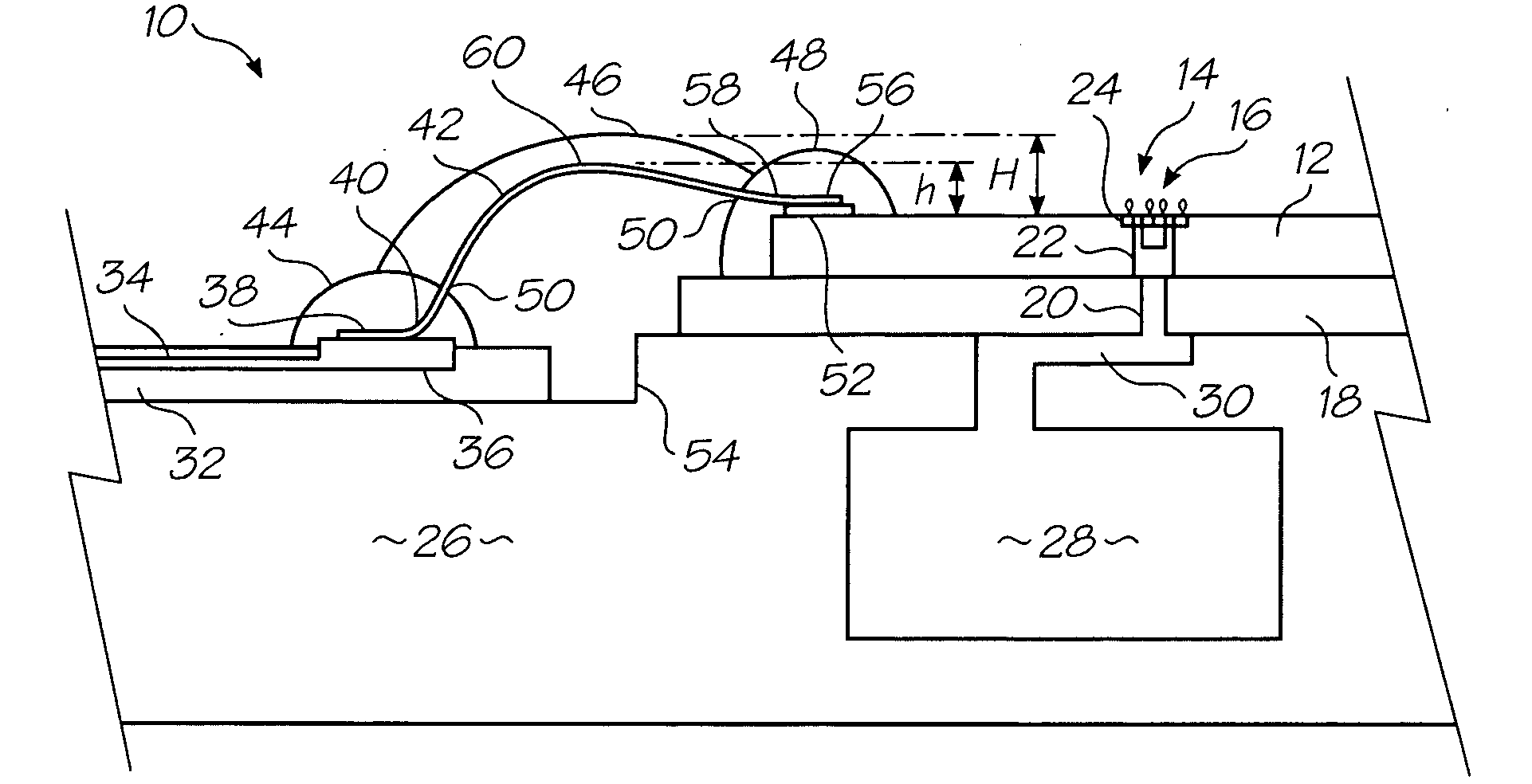
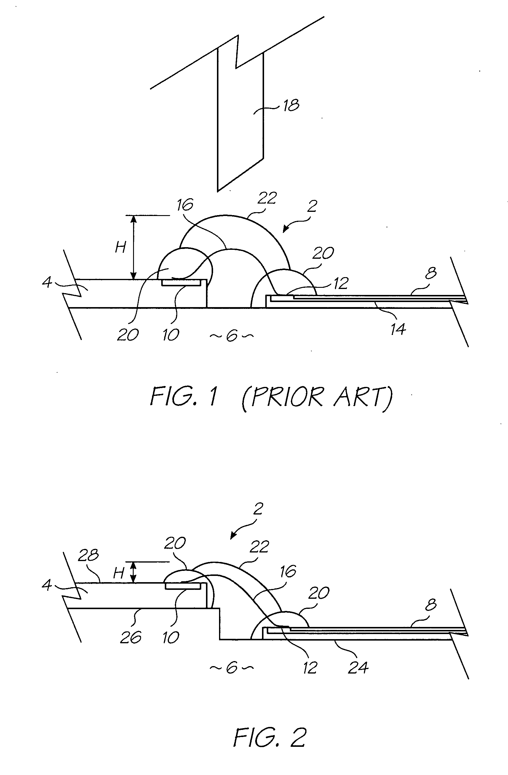
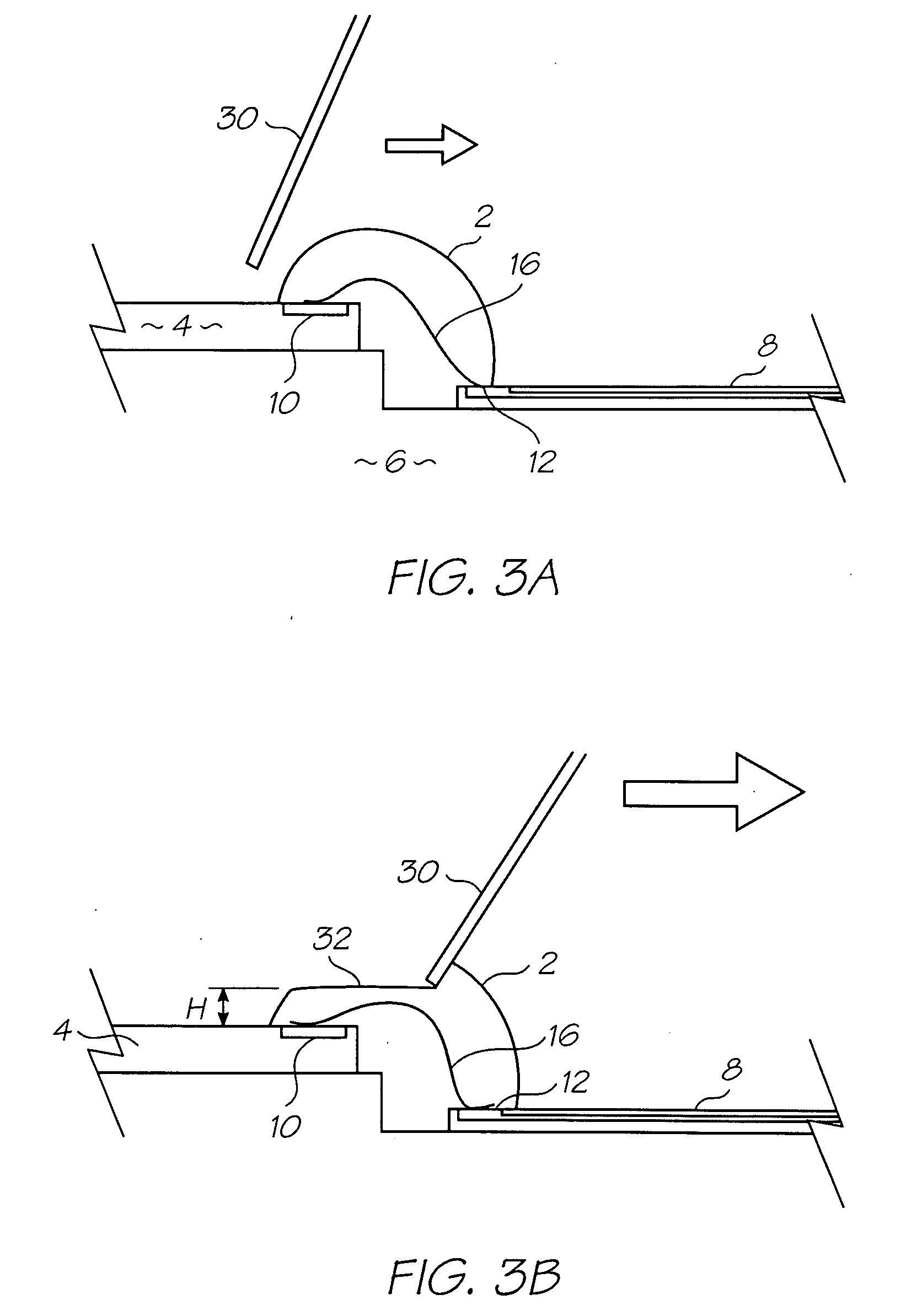
[0128]FIG. 1 shows a common technique used for applying a bead encapsulant to wire bonds. A die 4 is mounted to a supporting structure 6 adjacent the edge of a flex PCB 8 (flexible printed circuit board). The die 4 has a line of contact pads 10 along one edge and the flex PCB 8 has corresponding bond pads 12. Wire bonds 16 extend from the bond pads 10 to the bonds pads 12. Power and data is transmitted to the die 4 via conductive traces 14 in the flex PCB 8. This is a simplified representation of the dies mounted within many electronic devices. The printhead IC dies mounted to the LCP (liquid crystal polymer) molding to receive print data from an adjacent flex PCB, as described in U.S. Ser. No. 11 / 014,769 incorporated herein by cross reference, is one example of this type of die mounting arrangement. The ordinary worker will appreciate that the die may also be mounted directly to a hard PCB with traces formed thereon.

[0129]The wire bonds 16 are covered in a bead on encapsulant 2 to ...


PUM


Abstract

A method of forming an asymmetrical encapsulant bead on a series of wire bonds electrically connecting a micro-electronic device to a series of conductors, the micro-electronic device having a planar active surface. The method has the steps of positioning the die and the wire bonds beneath an encapsulant jetter that jets drops of encapsulant on to the wire bonds, the drops of encapsulant following a vertical trajectory, tilting the die such that the active surface is inclined to the horizontal and, jetting the drops of encapsulant to form a bead of encapsulant material covering the series of wire bonds, the bead having a cross sectional profile that is asymmetrical about an axis parallel to a normal to the active surface.

Description

CROSS REFERENCE TO RELATED APPLICATIONS[0001]The present application is a Continuation-In-Part of U.S. Ser. No. 12 / 237,390, filed Sep. 25, 2008, the contents of which are incorporated herein by cross reference.FIELD OF THE INVENTION[0002]The invention relates to the field of integrated circuit packaging. In particular, the encapsulation of the wire bonds between a circuit board and the contact pads on the integrated circuit die.BACKGROUND OF THE INVENTION[0003]Integrated circuits fabricated on silicon wafer substrates are electrically connected to printed circuit boards by wire bonds. The wire bonds are very thin wires—around 25 to 40 microns in diameter—extending from contact pads along the side of the wafer substrate to contacts on the printed circuit board (PCB). To protect and strengthen the wire bonds, they are sealed within a bead of epoxy called encapsulant. The wires from the contact pads to the PCB are made longer than necessary to accommodate changes in the gap between the...

Claims


Application Information

Patent Timeline
Patent Type & Authority Applications(United States)
IPC IPC(8): H01L21/00
CPCH01L21/56H01L2924/01033H01L24/78H01L24/85H01L2224/45015H01L2224/48091H01L2224/48227H01L2224/48472H01L2224/78H01L2224/85181H01L2224/8592H01L2224/85947H01L2924/01014H01L2924/01082H01L2924/09701H01L2924/14H01L2924/15153H01L2924/15165H01L2924/20753H01L24/48H01L2924/1461H01L2224/49175H01L2924/10253H05K2203/049H05K2201/09045H05K1/189H01L2924/00014H01L2924/00B41J2/14B41J2/16B41J2/1623B41J2002/14491H01L24/49H01L2224/85205H01L2224/45099H01L2924/20752H01L2924/20754H01L2224/05599
Inventor CHEW, NADINE LEE-YENPEREZ, ELMER DIMACULANGANTANKONGCHUMRUSKUL, KIANGKAI
Owner MEMJET TECH LTD
Why Eureka
Try Eureka