

Sputtering method and sputtering apparatus
- Summary
- Abstract
- Description
- Claims
- Application Information
AI Technical Summary
Benefits of technology
Problems solved by technology
Method used
Image

Examples
first embodiment
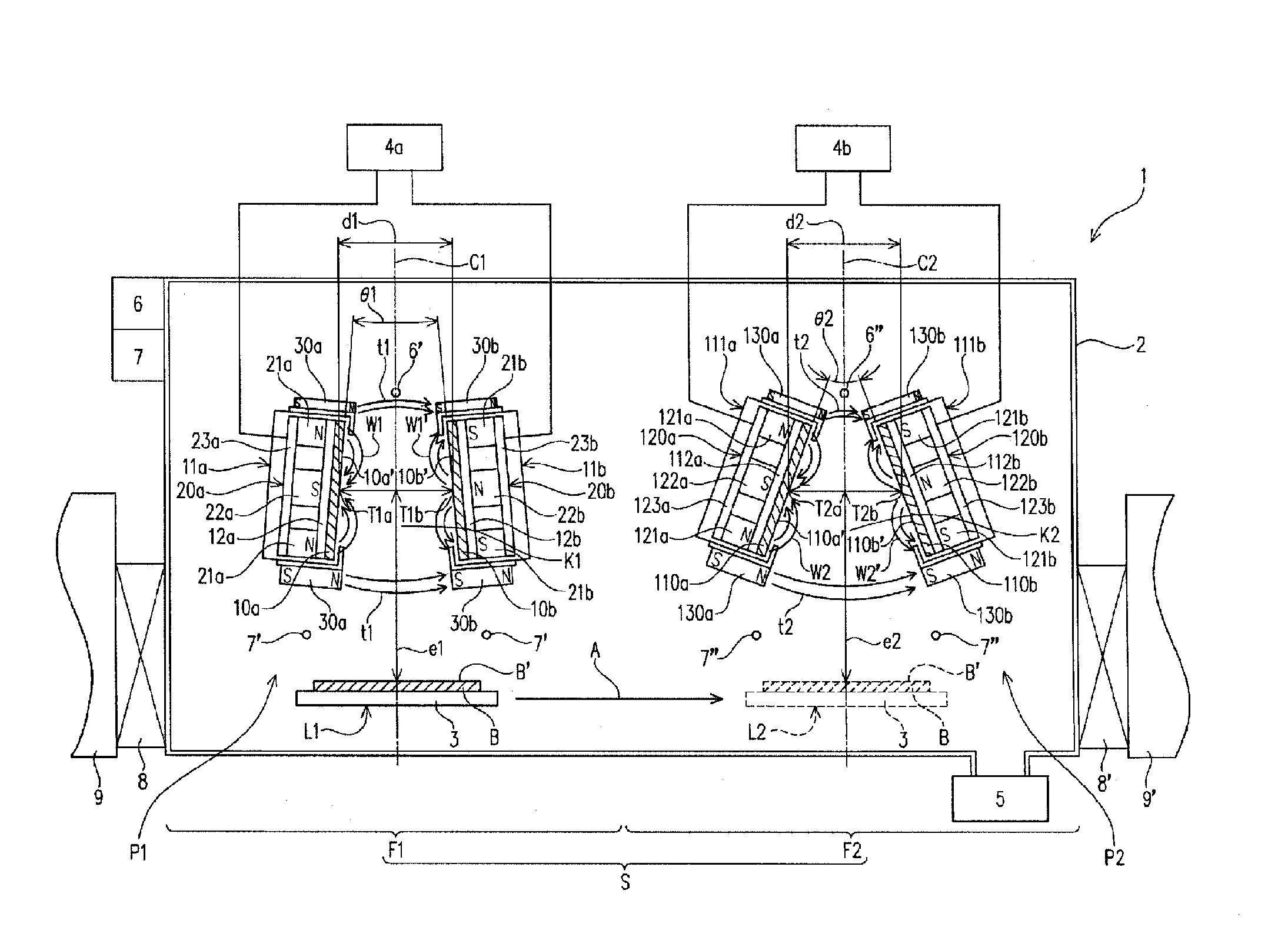
[0183]Hereinafter, the present invention will be described with reference to FIGS. 1 to 3.
[0184]As depicted in FIG. 1, a sputtering apparatus 1 includes a vacuum chamber 2 having an inner space S; a first film forming unit P1 and a second film forming unit P2 for forming a film on a film formation target surface B′ of a substrate B which is a target object on which a film is to be formed; and a holder (hereinafter, referred to as a substrate holder) 3 capable of moving inside the vacuum chamber 2 at least from a first film formation position L1, where a film formation is performed on the substrate B in the first film forming unit P1, to a second film formation position L2, where a film formation is performed on the substrate B in the second film forming unit P2 (moving in an arrow A direction), while holding the substrate B thereon.
[0185]Further, the sputtering apparatus 1 includes a first sputtering power supply 4a for supplying a sputtering power to the first film forming unit P1;...
second embodiment
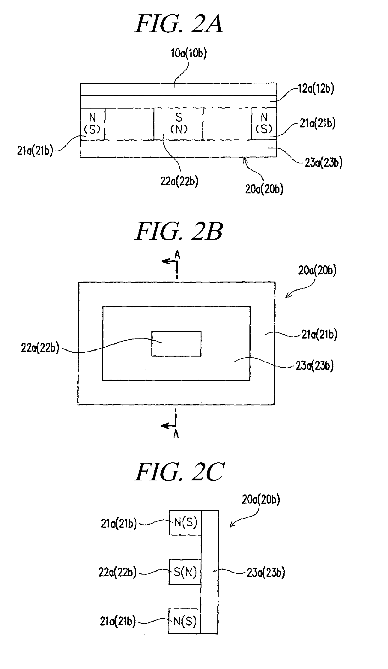
[0267]Moreover, in the second embodiment and other embodiments to be described later, a cathode in which a target surface of the magnetron cathode is arranged in parallel with the film formation target surface B′ of the substrate B may be referred to as “parallel plate type magnetron cathode”.
[0268]The second target 110′ in the present embodiment is made of ITO (Indium Tin oxide) in the same manner as in the first embodiment. Further, the second target 110′ is formed of a rectangular plate-shaped member having a size of about 125 mm (width)×300 mm (length)×5 mm (thickness). The second target 110′ is disposed such that it faces in parallel with the film formation target surface B′ of the substrate B when the substrate B is positioned at the second film formation position L′2 of the second film forming unit P′2 within the vacuum chamber 2, and its surface (surface to be sputtered) 110′a′ is spaced away from the film formation target surface B′ at a predetermined distance.
[0269]As desc...
third embodiment
[0297]Moreover, in the third embodiment, a pair of parallel plate type magnetron cathodes may be called “dual magnetron cathode” when they are arranged in juxtaposition such that their target surfaces are on the same plane in the same direction, and parallel plate type magnetron cathodes are connected with an AC power supply having a phase difference of about 180°, which will be described later.
[0298]The second target 110″a (110″b) in the present embodiment is made of ITO (Indium Tin Oxide) in the same manner as in the first embodiment. Further, the second target 110″a (110″b) is formed of a rectangular plate-shaped member having a size of about 125 mm (width)×300 mm (length)×5 mm (thickness). In addition, the second target 110″a (110″b) is disposed such that it faces parallel or substantially parallel to the film formation target surface B′ of the substrate B (facing slightly toward the substrate B) when the substrate B is positioned at the second film formation position L″2 of the...
PUM
| Property | Measurement | Unit |
|---|---|---|
| Time | aaaaa | aaaaa |
| Angle | aaaaa | aaaaa |
| Temperature | aaaaa | aaaaa |
Abstract
Description
Claims
Application Information