

Method and structure for adhesion of absorber material for thin film photovoltaic cell
a photovoltaic cell and absorber material technology, applied in the field of photovoltaic materials and manufacturing methods, can solve the problems of reducing the adhesion of absorber materials to the surface of the absorber material, etc., to achieve the effect of less toxic and convenient bonding to the electrode structur
- Summary
- Abstract
- Description
- Claims
- Application Information
AI Technical Summary
Benefits of technology
Problems solved by technology
Method used
Image

Examples
Embodiment Construction
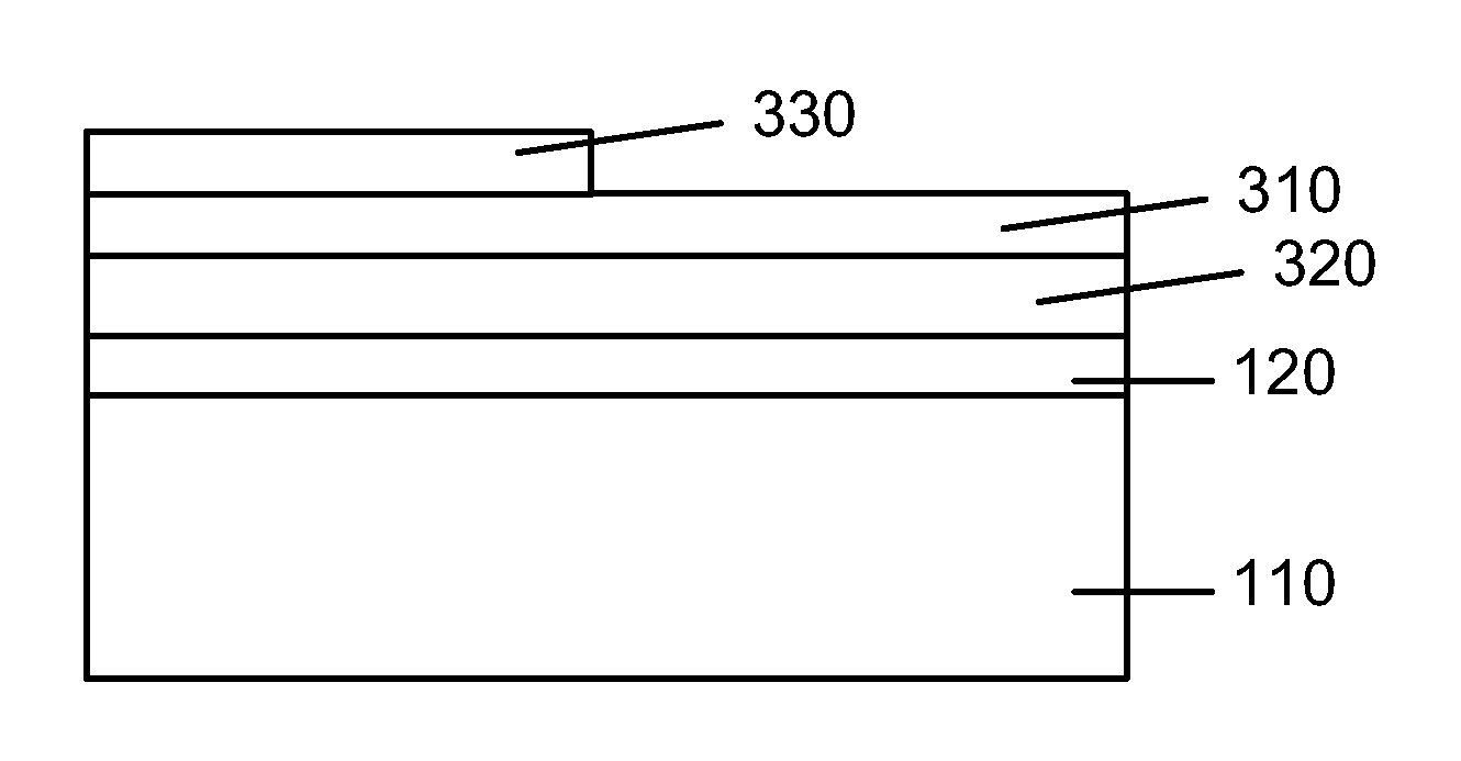
[0011]According to embodiments of the present invention, a method and a structure for forming semiconductor materials for photovoltaic applications are provided. More particularly, the present invention provides a method and structure using a material facilitating adhesion between an absorber material and electrode material for manufacture of high efficiency thin film photovoltaic cells. But it would be recognized that the present invention has a much broader range of applicability, for example, embodiments of the present invention may be used to form other semiconducting thin films or multilayers comprising iron sulfide, cadmium sulfide, zinc selenide, and others, and metal oxides such as zinc oxide, iron oxide, copper oxide, and others.
[0012]In a specific embodiment, a method according to an embodiment of the present invention is outlined below.
[0013]1. Start;
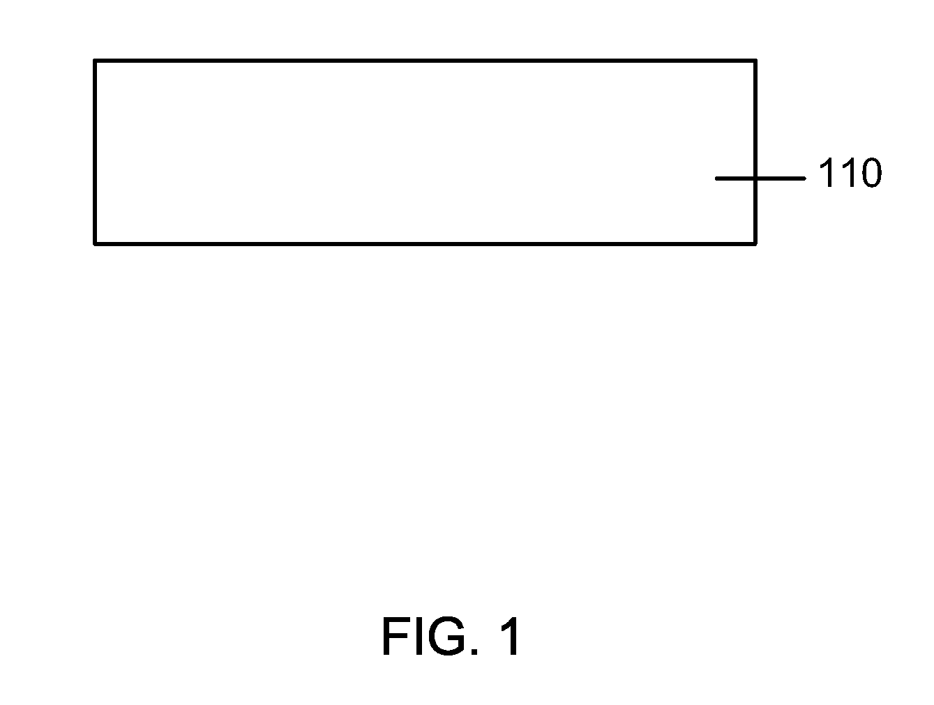
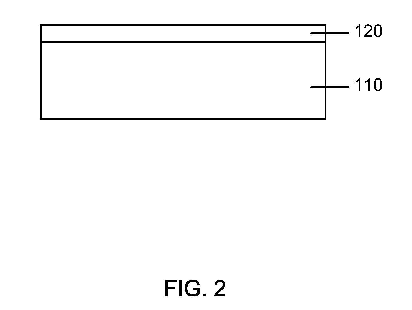
[0014]2. Provide a transparent substrate comprising a surface region;
[0015]3. Form a first electrode layer overlying the su...
PUM
| Property | Measurement | Unit |
|---|---|---|
| thickness | aaaaa | aaaaa |
| thickness | aaaaa | aaaaa |
| thickness | aaaaa | aaaaa |
Abstract
Description
Claims
Application Information