Secure memory interface

Active Publication Date: 2010-04-01
SAMSUNG ELECTRONICS CO LTD
View PDF4 Cites 46 Cited by
  • Summary
  • Abstract
  • Description
  • Claims
  • Application Information

AI Technical Summary

Benefits of technology

[0030]In this manner, the CPU flexibly specifies the amount and location of the data stored into the memory device with secure access. Fault injection is detected for such data as specified by the CPU using the reader and writer blocks implemented in hardware i

Problems solved by technology

Memory devices are prone to fault injection attacks such as by use of lasers or X-rays.
However, the laser detector is not adapted to detect for laser attacks on memory devices.
However, implementation of such error detection code within the memory devices increases the silicon area of the memory device.
In addition, if the states of the bits are modified on a bus outside of the memory device, the error detection code

Method used


Image

  • Secure memory interface
  • Secure memory interface
  • Secure memory interface

Examples


Embodiment Construction

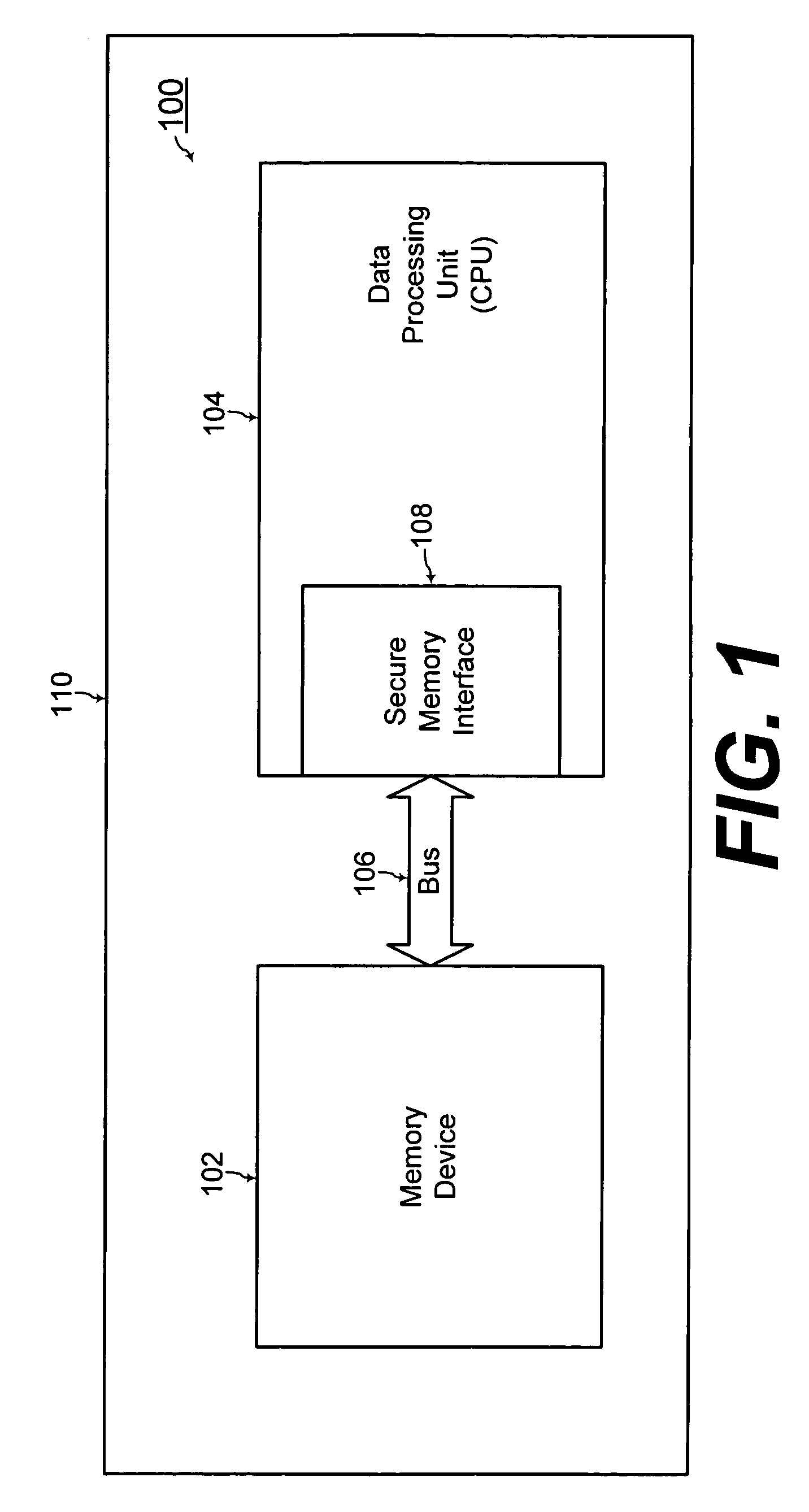
[0050]FIG. 1 shows a block diagram of an electronic system 100 having a memory device 102, a data processing unit 104, and a bus 106. The electronic system 100 may be formed as components of a smart card 110 in an example embodiment of the present invention. However, the present invention is not limited thereto, and the present invention may be practiced with the electronic system 100 being in other applications. The present invention may be practiced with the memory device 102 and the data processing unit 104 being fabricated as one integrated circuit chip, or being fabricated as two separate integrated circuit chips.

[0051]The memory device 102 and the data processing unit 104 exchange signals via the bus 106. The data processing unit 104 is a CPU (central processing unit) with a secure memory interface 108 (i.e., an interface unit) in an example embodiment of the present invention.

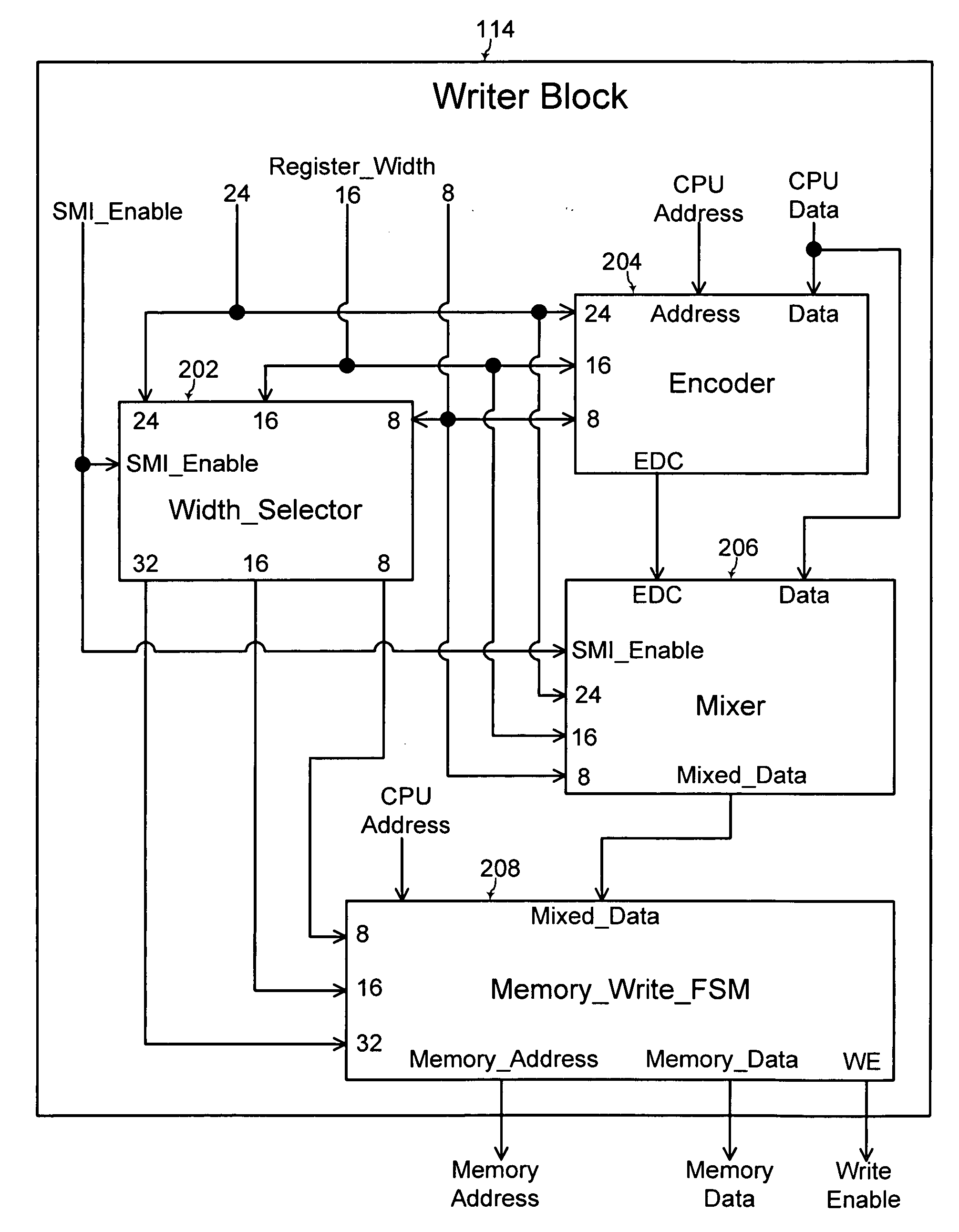
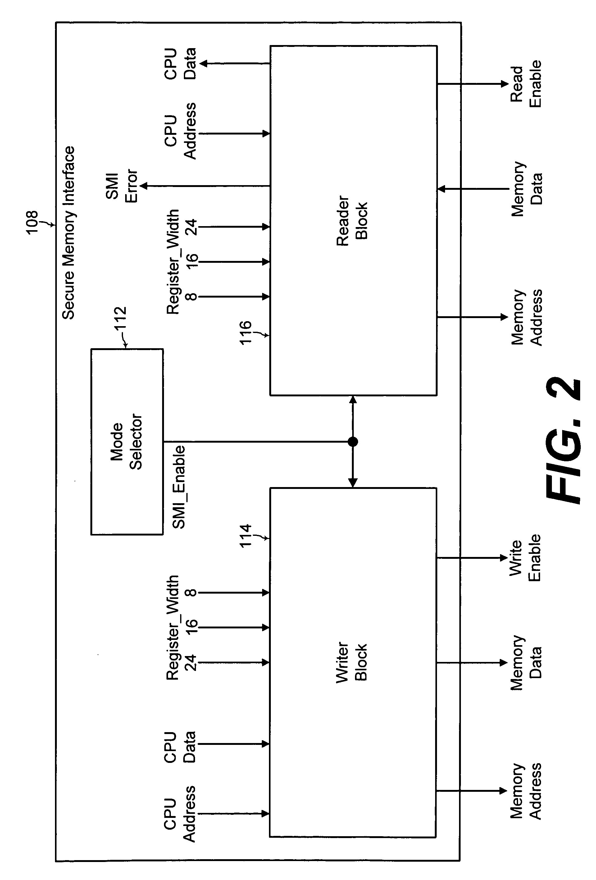
[0052]Referring to FIGS. 1 and 2, the secure memory interface 108 includes a mode selector 112, a wri...


PUM


Abstract

A secure memory interface includes a reader block, a writer block, and a mode selector for detecting fault injection into a memory device when a secure mode is activated. The mode selector activates or deactivates the secure mode using memory access information from a data processing unit. Thus, the data processing unit flexibly specifies the amount and location of the secure data stored into the memory device.

Description

CROSS-REFERENCE TO RELATED APPLICATION(S)[0001]The present application claims priority under 35 U.S.C. §119 to Korean Patent Application No. 2008-0096574, filed on Oct. 1, 2008, which is incorporated herein by reference in its entirety.TECHNICAL FIELD [0002]The present invention relates generally to electronic systems with a memory device and a data processing unit, and more particularly, to flexible control of secure or regular access to the memory device by the data processing unit.BACKGROUND OF THE INVENTION [0003]Memory devices are prone to fault injection attacks such as by use of lasers or X-rays. For example, lasers and X-rays allow for precise attacks by modifying states of bits in the memory device. The laser is especially suitable for injecting faults in registers, RAM (random access memory) devices, EEP (electrically erasable and programmable) memory devices, and flash memory devices. Such fault injection may be permanent or temporary.[0004]In addition, such fault injecti...

Claims


Application Information

Patent Timeline
IPC IPC(8): G06F12/14
CPCG06F12/1433G06F21/74G06F12/14G06F21/85G06F2221/2105G06F21/79G06F11/08G06F15/00G06F21/00
Inventor RIOU, SEBASTIEN
Owner SAMSUNG ELECTRONICS CO LTD
Why Eureka
Try Eureka