Touch panel and method for driving the same

a technology of touch panel and display screen, which is applied in the field of touch panel, can solve the problems of deteriorating display quality and difficulty in accurately reading the object to be detected, and achieve the effects of improving spatial resolution, high-sensitivity detection, and high-sensitivity detection

Active Publication Date: 2010-04-08
SEMICON ENERGY LAB CO LTD
View PDF15 Cites 33 Cited by
  • Summary
  • Abstract
  • Description
  • Claims
  • Application Information

AI Technical Summary

Benefits of technology

[0021]Even with a touch panel provided with a photo sensor in a pixel, high-sensitivity detection can be achieved.
[0022]The above structure enables a touch panel which can perform high-sensitivity detection to be achieved and spatial resolution to be improved, thereby improving reading accuracy of an object to be detected. Further, since the aperture ratio is not reduced, the reading accuracy of the touch panel can be improved without lowering display quality.
[0023]Accordingly, the object to be detected can be read accurately in detail. Therefore, finger print authentication or the like can be conducted on the touch panel, and the object to be detected can be identified without providing other equipment.

Problems solved by technology

In a conventional case, for example, when an optical touch sensor (photo sensor) is provided in a touch panel capable of color display, non-uniformity is caused in the hue of light which is reflected by an object to be detected; therefore, it was difficult to accurately read the object to be detected.
However, when the integration degree of the touch sensors is increased, an aperture ratio of a display device is lowered, which leads to deterioration in display quality.

Method used


Image

  • Touch panel and method for driving the same
  • Touch panel and method for driving the same
  • Touch panel and method for driving the same

Examples


embodiment

[0032]Hereinafter, a touch panel which is one embodiment of the present invention and a driving method thereof will be described.

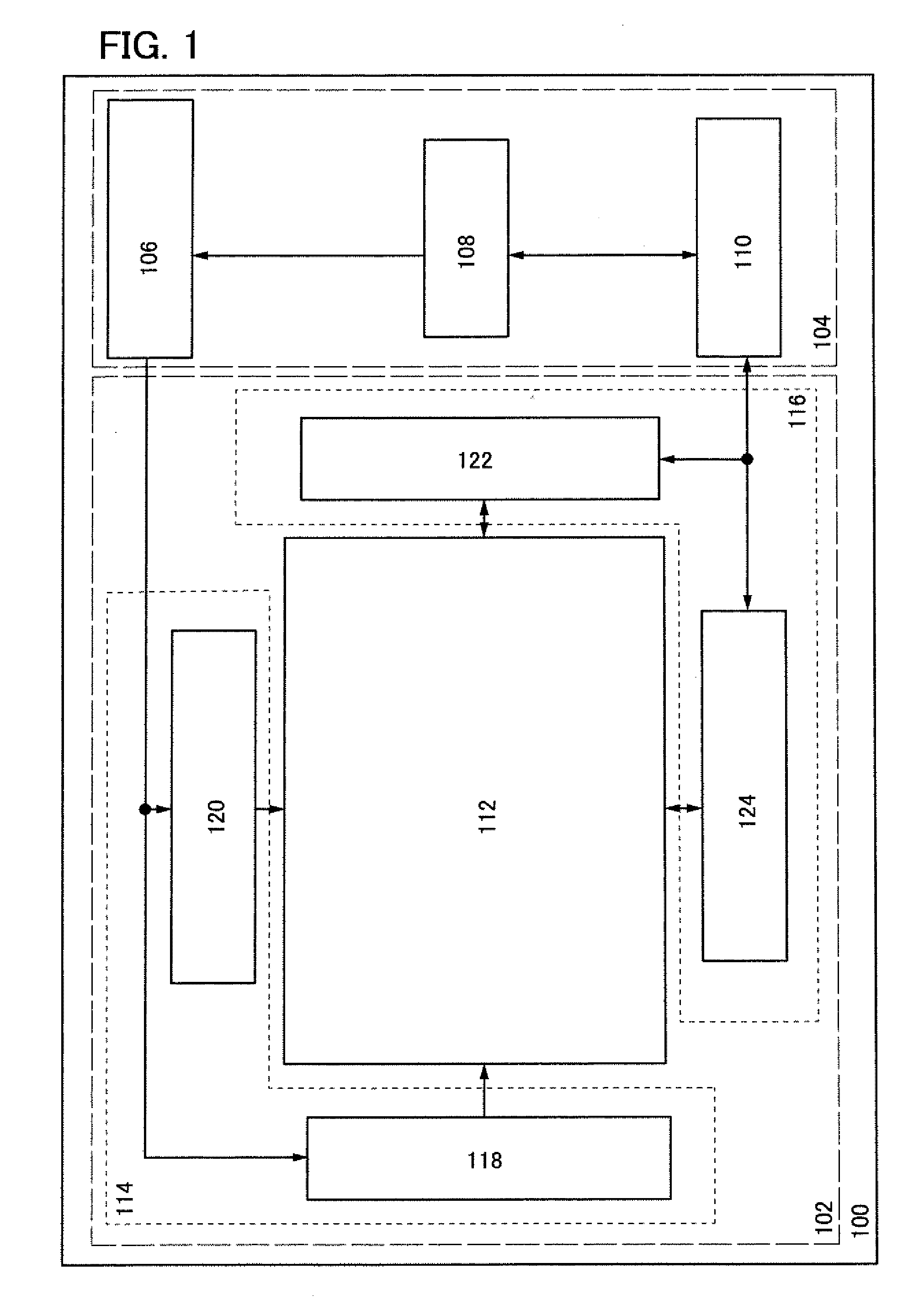
[0033]FIG. 1 is a block diagram illustrating an example of the structure of the touch panel which is one embodiment of the present invention. A touch panel 100 illustrated in FIG. 1 includes a display portion 102 and an arithmetic control circuit portion 104.

[0034]The arithmetic control circuit portion 104 includes a display element control circuit 106, an arithmetic circuit 108, and a sensor control circuit 110.

[0035]The display portion 102 includes a pixel circuit 112, a display element driver circuit 114, and a sensor driver circuit 116.

[0036]The display element control circuit 106 has a function of generating a signal for controlling the display element driver circuit 114 using a signal transmitted from the arithmetic circuit 108 and supplying the signal to the display element driver circuit 114.

[0037]The arithmetic circuit 108 has a function of genera...

example 1

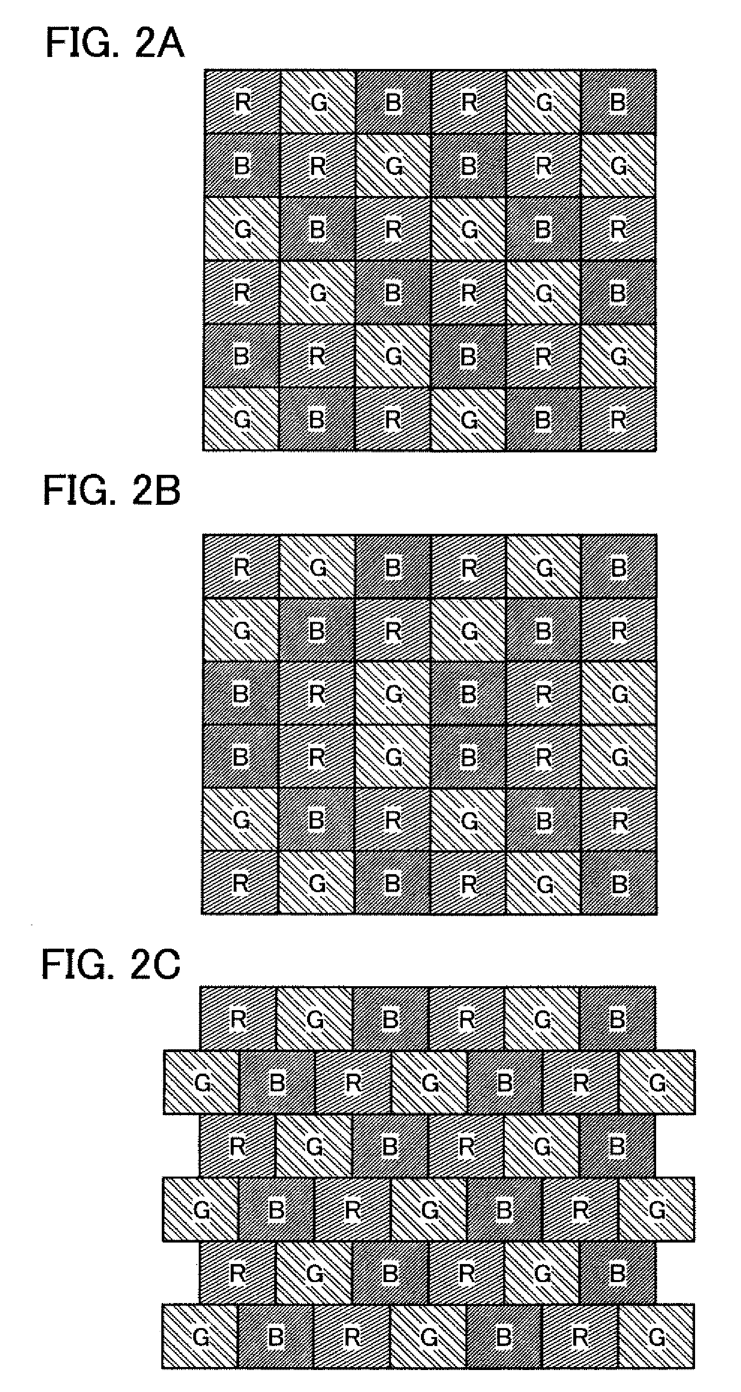
[0065]In this example, an example of a touch panel including a liquid crystal element will be described with reference to FIG. 5 as one preferable mode of the touch panel. FIG. 5 is a cross-sectional view in a state in which a finger 135 as an object to be detected is in contact with a display portion of a touch panel.

[0066]As a substrate 150, a light-transmitting substrate such as a glass substrate or a quartz substrate is used. Over the substrate 150, at least a thin film transistor 151, a thin film transistor 152, and a photo sensor 153 are provided. The thin film transistor 151 is connected to the photo sensor 153, and the thin film transistor 152 is connected to a liquid crystal element. The photo sensor 153 is formed by a stack of an n-type semiconductor layer 160, an i-type semiconductor layer 161, and a p-type semiconductor layer 162. The n-type semiconductor layer 160 contains an impurity element imparting n-type conductivity (e.g., phosphorus). The i-type semiconductor lay...

example 2

[0091]In this example, an electronic device to which the touch panel described in the above embodiment and example is applied and an application of the electronic device will be described.

[0092]FIG. 6A illustrates a monitor type touch panel which is one embodiment of the present invention. The monitor type touch panel illustrated in FIG. 6A includes a chassis 176, a display portion 177, a support 178, and the like. The touch panel which is one embodiment of the present invention is incorporated in the chassis 176, and a photo sensor is provided in a pixel of the display portion 177. The display portion 177 has a display function and an information input function. With the use of the touch panel which is one embodiment of the present invention, high-sensitivity detection can be performed, thereby obtaining a monitor type touch panel with high accuracy in reading.

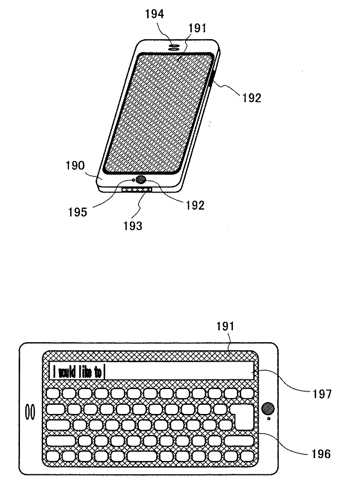
[0093]FIG. 68 illustrates a portable game machine to which the touch panel which is one embodiment of the present invention...


PUM


Abstract

A touch panel having high reading accuracy of an object to be detected is provided. In a method for driving a touch panel which is provided with a photo sensor in a pixel, an image is displayed in a display portion of a touch panel, a detection region is determined by detecting approach or contact of an object to be detected in a state in which the image is displayed, and the object to be detected is read while substantially equalizing the intensity of light of pixels in the detection region per unit time and unit area. The intensity of light of the pixels per unit time and unit area, which is to be substantially equal, is preferably the maximum intensity of light in the detection region before adjustment, more preferably, the intensity of light for white display.

Description

BACKGROUND OF THE INVENTION[0001]1. Field of the Invention[0002]The present invention relates to a touch panel which is formed using a touch sensor and a method for driving the touch panel. In particular, the present invention relates to a touch panel in which pixels provided with touch sensors are arranged in matrix and a method for driving the touch panel. Further, the present invention relates to a semiconductor device and an electronic device including the touch sensor.[0003]2. Description of the Related Art[0004]In recent years, a display device provided with a touch sensor has attracted attention. The display device provided with a touch sensor is called a touch panel, a touch screen, or the like (hereinafter referred to as a touch panel). Examples of the touch sensor include a resistive touch sensor and a capacitive touch sensor, which are different in operation principle. In both kinds of sensors, data can be input by contact of an object to be detected with a display portio...

Claims


Application Information

Patent Timeline
Patent Type & Authority Applications(United States)
IPC IPC(8): G06F3/042G09G3/36
CPCG06F1/1616G06F1/1626G06F3/042G06F3/03547G06F3/0412G06F1/1643
Inventor KUROKAWA, YOSHIYUKIIKEDA, TAKAYUKI
Owner SEMICON ENERGY LAB CO LTD
Why Eureka
Try Eureka