Method for gate height control in a gate last process

a gate height and gate technology, applied in the field of gate height control in the gate last process, can solve the problems of exacerbated problems, problems such as the inability to implement such features and processes, and the inability to control the gate heigh

Inactive Publication Date: 2010-04-08
TAIWAN SEMICON MFG CO LTD
View PDF3 Cites 28 Cited by
  • Summary
  • Abstract
  • Description
  • Claims
  • Application Information

AI Technical Summary

Benefits of technology

[0006]Yet another one of the broader forms of an embodiment of the present invention involves a method of fabricating a semiconductor device. The method includes providing a semiconductor substrate; forming a transistor having a gate stack disposed on the substrate, the gate stack including an interfacial layer, a high-k dielectric layer, a dummy poly gate; forming an inter-layer dielectric (ILD) over the substrate and the transistor; planarizing the ILD to expose a top surface of the dum

Problems solved by technology

There are challenges to implementing such features and processes in CMOS fabrication however.
As the gate lengths decrease, these problems are exacerbated.
For example, in a “gate last” fabr

Method used


Image

  • Method for gate height control in a gate last process
  • Method for gate height control in a gate last process
  • Method for gate height control in a gate last process

Examples


Embodiment Construction

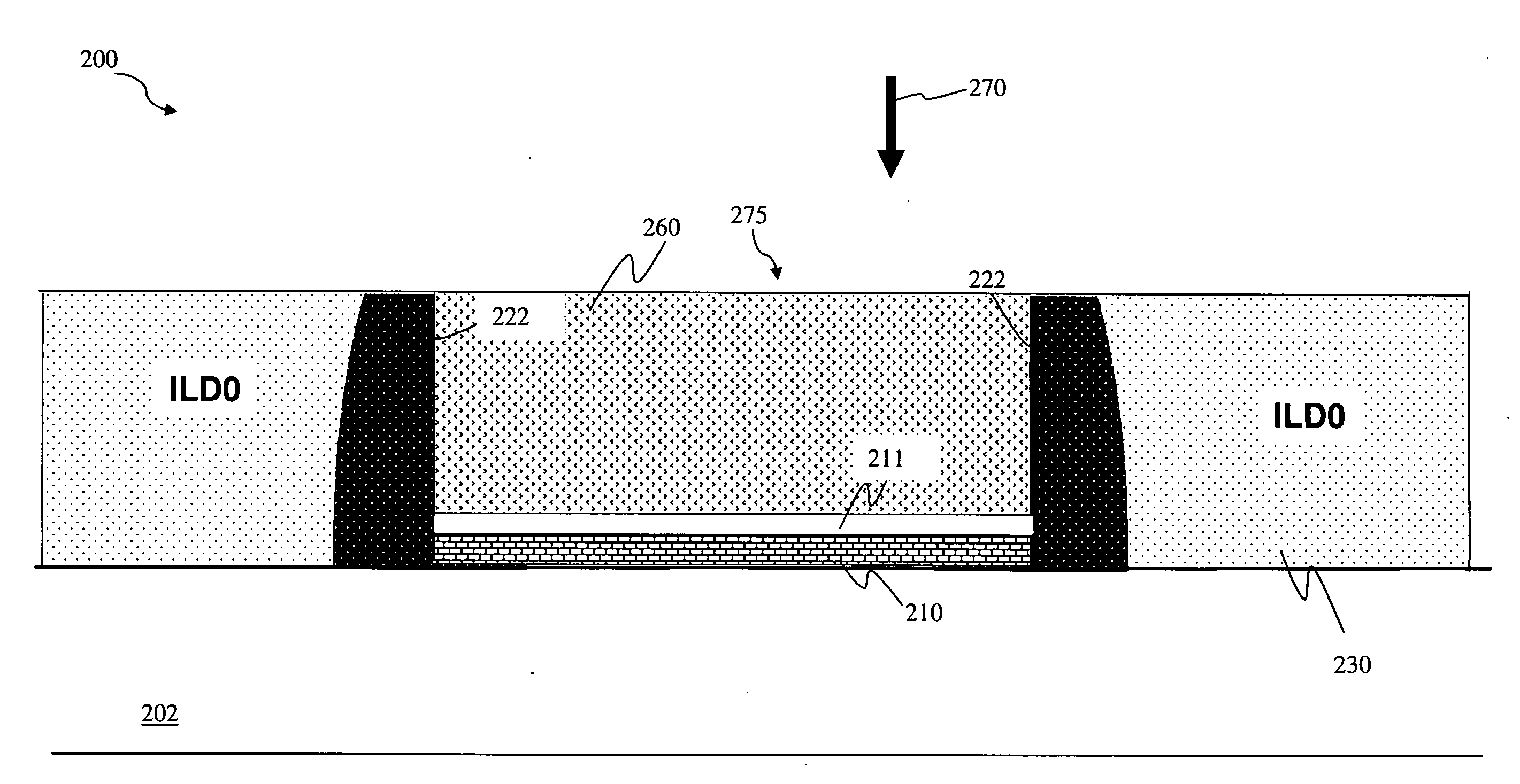
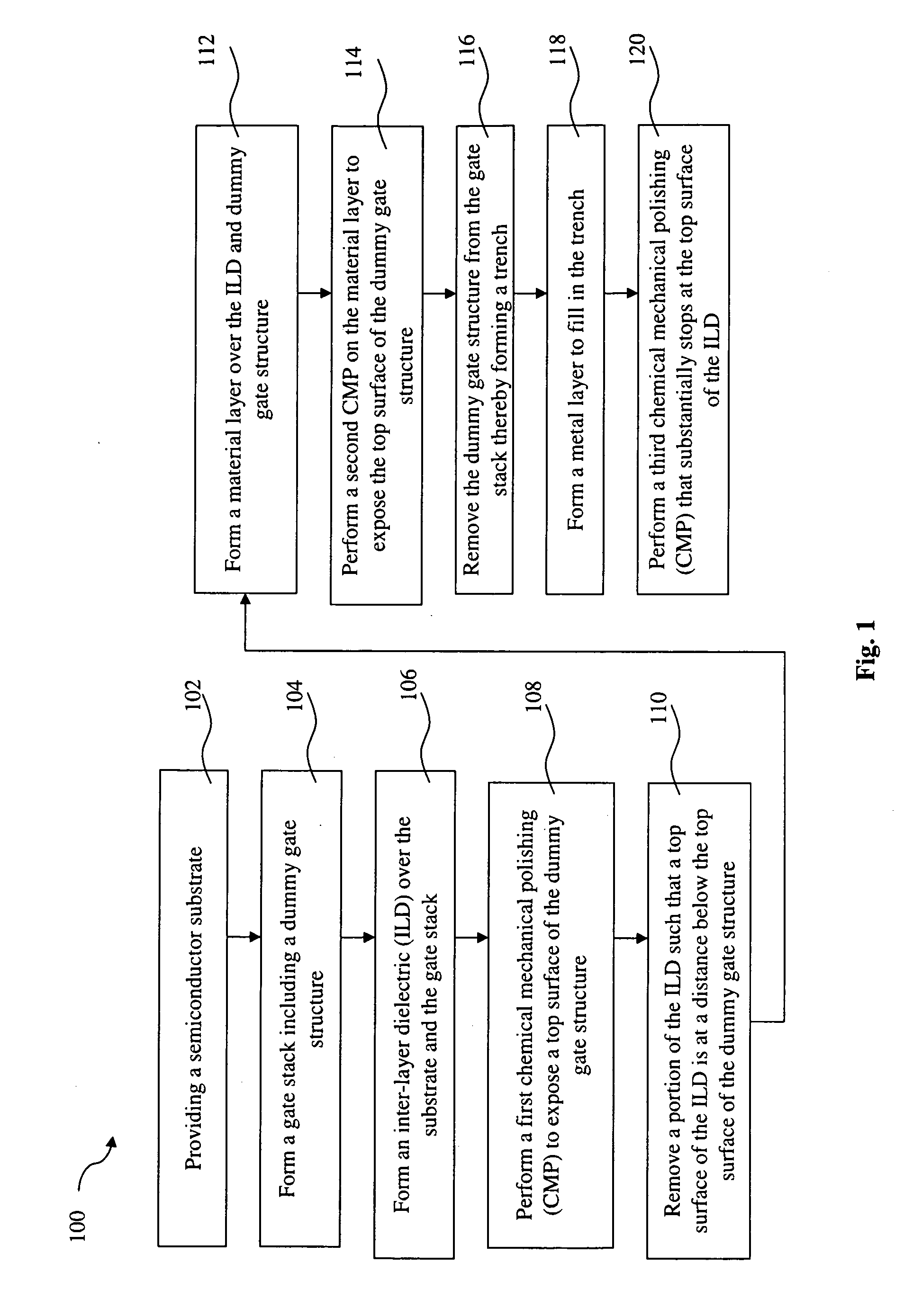
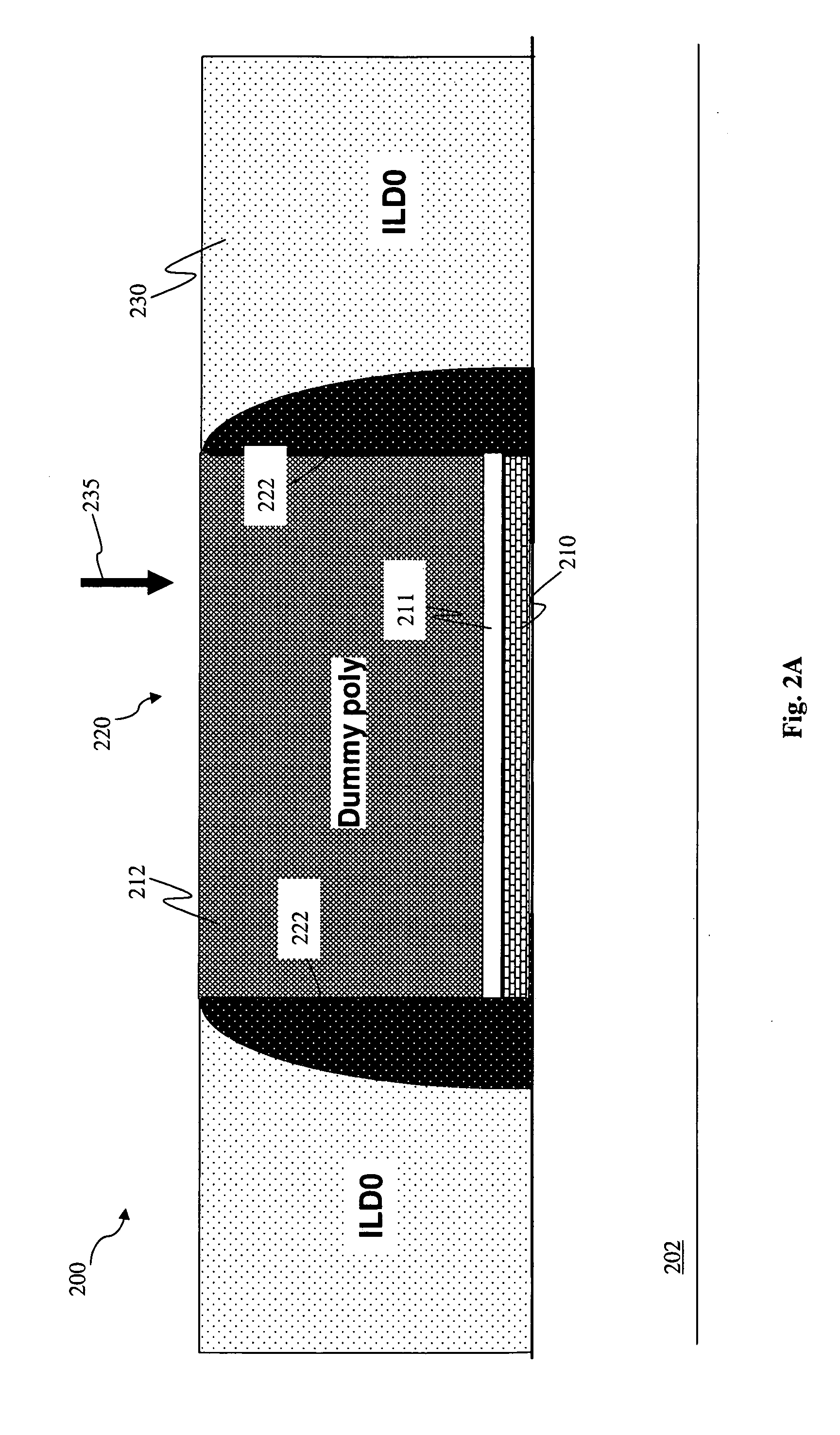
[0010]The present disclosure relates generally to forming an integrated circuit device on a substrate and, more particularly, to fabricating a gate structure as part of an integrated circuit (including FET devices). It is understood, however, that the following disclosure provides many different embodiments, or examples, for implementing different features of the invention. Specific examples of components and arrangements are described below to simplify the present disclosure. These are, of course, merely examples and are not intended to be limiting. In addition, the present disclosure may repeat reference numerals and / or letters in the various examples. This repetition is for the purpose of simplicity and clarity and does not in itself dictate a relationship between the various embodiments and / or configurations discussed. In addition, the present disclosure provides examples of a “gate last” metal gate process, however one skilled in the art may recognize applicability to other pro...


PUM


Abstract

A method is provided for fabricating a semiconductor device that includes providing a semiconductor substrate, forming a transistor in the substrate, the transistor having a gate structure that includes a dummy gate structure, forming an inter-layer dielectric (ILD), performing a first chemical mechanical polishing (CMP) to expose a top surface of the dummy gate structure, removing a portion of the ILD such that a top surface of the ILD is at a distance below the top surface of the dummy gate structure, forming a material layer over the ILD and dummy gate structure, performing a second CMP on the material layer to expose the top surface of the dummy gate structure, removing the dummy gate structure thereby forming a trench, forming a metal layer to fill in the trench, and performing a third CMP that substantially stops at the top surface of the ILD.

Description

PRIORITY DATA[0001]This application claims priority to Provisional Application Ser. No. 61 / 102,968 filed on Oct. 6, 2008, entitled “Method For Gate Height Control In A Gate Last Process,” the entire disclosure of which is incorporated herein by reference.BACKGROUND[0002]As technology nodes shrink, in some IC designs, there has been a desire to replace the typically polysilicon gate electrode with a metal gate electrode to improve device performance with the decreased feature sizes. Providing metal gate structures (e.g., including a metal gate electrode rather than polysilicon) offers one solution. One process of forming a metal gate stack is termed “gate last” process in which the final gate stack is fabricated “last” which allows for reduced number of subsequent processes, including high temperature processing, that must be performed after formation of the gate. Additionally, as the dimensions of transistors decrease, the thickness of the gate oxide must be reduced to maintain perf...

Claims


Application Information

Patent Timeline
IPC IPC(8): H01L21/28
CPCH01L21/28088H01L29/4966H01L29/78H01L29/513H01L29/66545H01L29/51
Inventor CHUNG, SHENG-CHENTHEI, KONG-BENGCHUANG, HARRY
Owner TAIWAN SEMICON MFG CO LTD
Why Eureka
Try Eureka