Stress micro mechanical test cell, device, system and methods

a micro-mechanical test cell and micro-cell technology, applied in the field of nanofiber testing and micro-devices, can solve the problems of not being able to meet the standards of testing and materials, not being able to test the mechanical properties of nanofibers, and lacking practical testing methods and apparatuses that fit within the nanofiber manufacturing schem

Active Publication Date: 2010-04-08
THE BOARD OF TRUSTEES OF THE UNIV OF ILLINOIS
View PDF10 Cites 31 Cited by
  • Summary
  • Abstract
  • Description
  • Claims
  • Application Information

AI Technical Summary

Problems solved by technology

Determining nanofiber mechanical properties is not a straightforward task, primarily due to their very small dimensions and fragility.
Practical testing methods and apparatuses that fit within the nanofiber manufacturing scheme are lacking.
Such testing techniques also fail to conform to standard set by the American Society for Testing and Materials) (ASTM).
Both the AFM cantilever and the SEM microscope place substantial limits on such tension testing techniques.
Since the AFM is used to create displacement and as the force sensor, relative error is increasing when the stiffness of the cantilever is substantially different than that of the nanofibers being tested.
Using an SEM is cumbersome, and use of an optical microscope is difficult due to the limited depth of field and the associated out-of-plane motion of the AFM cantilevers.
These devices have also had a limited range of force and displacement and are, therefore, poorly suited for use with strong and/or elastic nanofibers, some of which stretch by several tens of microns.
Nanoindentation lacks great accuracy due to uncertainties regarding the nanoindenter tip shape and the relative tip-fiber configuration, the effect of fiber surface curvature and roughness, and the adhesion force between the sample and the indenter.
The local measurement provided by indentation is a poor predicto

Method used


Image

  • Stress micro mechanical test cell, device, system and methods
  • Stress micro mechanical test cell, device, system and methods
  • Stress micro mechanical test cell, device, system and methods

Examples


Embodiment Construction

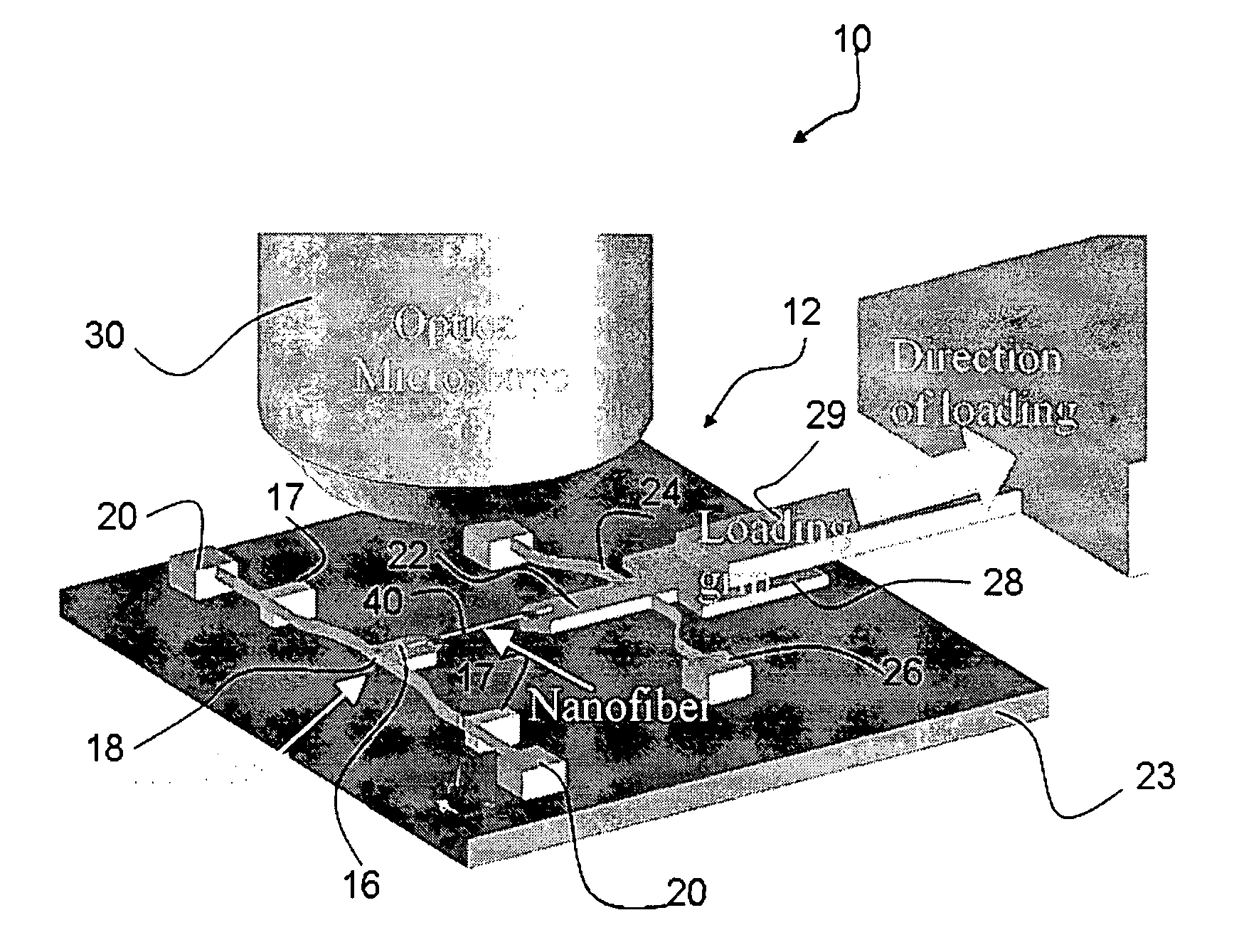
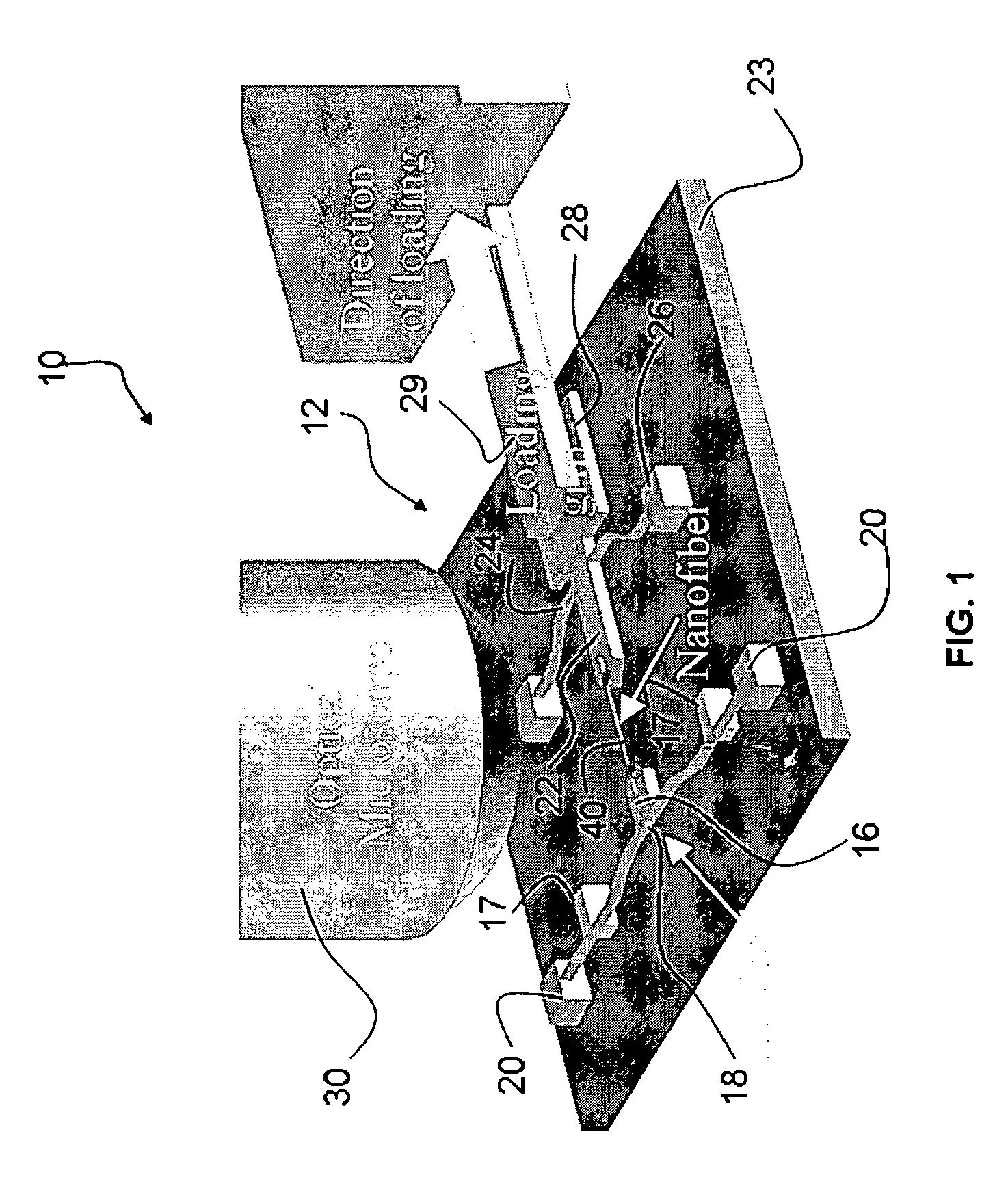
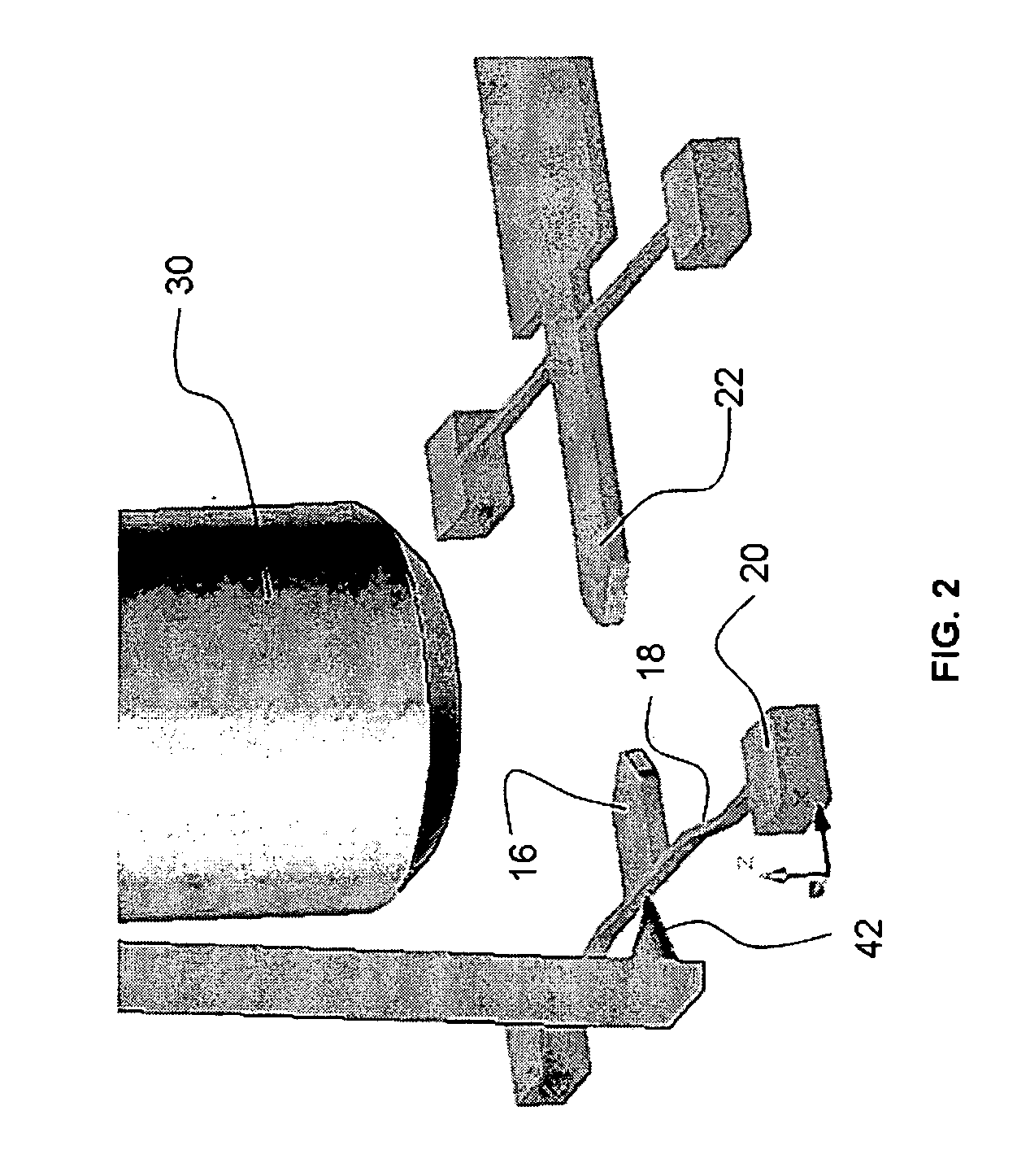
[0020]The invention provides micromechanical test cell, test system and testing methods. Embodiments of the invention are useful, for example for testing mechanical properties and adhesion testing of single nano- and micro-fibers at various loading rates, as well as for testing of nanowires and nanotubes.

[0021]An embodiment of the invention is a system for testing. The system includes a test cell in the form of a stress micro device formed by MEMS fabrication. The test cell is configured to apply stress to a nano- or micro-fiber, tube or wire. The motion of substantial portions of surfaces of the stress micro device is captured by an optical microscope with a high magnification objective in combination and analyzed with a digital image correlation algorithm. Data acquired during testing are analyzed to provide mechanical properties and / or adhesion properties of the elongated nano- or micro-sample being tested.

[0022]A test cell of the invention is useful for measuring stress and stra...


PUM

PropertyMeasurementUnit
Stiffnessaaaaaaaaaa
Stress optical coefficientaaaaaaaaaa

Abstract

The invention provides a stress micro mechanical system for measuring stress and strain in micro- and nano-fibers tubes, and wires as well as for measuring the interface adhesion force and stress in nanofibers and nanotubes embedded in a polymer matrix. A preferred system of the invention has a substrate for supporting a MEMS fabrication. The MEMS fabrication includes freestanding sample attachment points that are movable in a translation direction relative to one another when the substrate is moved and a sample is attached between the sample attachment points. An optical microscope images surfaces of the MEMS fabrication. Software conducts digital image correlation on obtained images to determine the movement of the surfaces at a resolution much greater than the hardware resolution of the optical microscope. A preferred method for measuring stress and strain in micro- and nano-fibers, tubes, and wires, and/or measuring the force required to pull-out individual micro- and nano-fibers, tubes, and wires from a polymer matrix and to therefore measure interfacial adhesion is also provided. In the method a sample is attached between freestanding platforms in a MEMS device. Relative translational movement between the platforms is created and motion of the platforms is imaged with an optical microscope. Mechanical and adhesion properties of the sample are determined by applying a digital image correlation algorithm to the image data.

Description

PRIORITY CLAIM AND REFERENCE TO RELATED APPLICATION[0001]The application claims priority under 35 U.S.C. §119 from prior provisional application Ser. No. 60 / 902,424, which was filed Feb. 21, 2007.STATEMENT OF GOVERNMENT INTEREST[0002]This invention was made with government support under[0003]Contract DMI 0532320 awarded by National Science Foundation. The government has certain rights in the invention.FIELD[0004]A field of the invention is materials testing, and particularly nanofiber testing. Another field of the invention is micro devices, and particularly micro elecromechanical devices (MEMS).BACKGROUND[0005]Polymeric nanofibers are an emerging class of building block materials with applications in tissue engineering, filtration and nanocomposites. They are fabricated by a number of different processes, all of which can produce significant batch to batch differences. These fabrication processes include drawing, template synthesis, and electrospinning. Slight variations in the fab...

Claims


Application Information

Patent Timeline
IPC IPC(8): G01Q60/24
CPCG01N19/04G01N2203/0286Y10T428/2976D02G3/22D01D5/0007
Inventor CHASIOTIS, IOANNISNARAGHI, MOHAMMAD
Owner THE BOARD OF TRUSTEES OF THE UNIV OF ILLINOIS
Why Eureka
Try Eureka