Semiconductor device, manufacturing method thereof, and manufacturing method of semiconductor module

a semiconductor module and semiconductor technology, applied in the direction of printed circuit aspects, sustainable manufacturing/processing, final product manufacturing, etc., to achieve the effect of improving the yield of mounting the semiconductor device and improving the reliability of the semiconductor devi

Inactive Publication Date: 2010-04-15
RENESAS ELECTRONICS CORP
View PDF15 Cites 31 Cited by
  • Summary
  • Abstract
  • Description
  • Claims
  • Application Information

AI Technical Summary

Benefits of technology

[0023]According to the representative embodiments, the reliability of the semiconductor device c

Problems solved by technology

First, when the BGA is mounted on a mounting substrate (motherboard), the bump electrodes (solder bumps) provided as the external terminals of the BGA are molten by performing a heat treatment thereto, and electrically coupled to the substrate terminals of the mounting substrate (referred to also as solder reflow). At this time, the thermal expansion coefficient of a semiconductor chip mounted on the wiring substrate (resin substrate with multilayer wiring or interposer), the thermal expansion coefficient of the wiring substrate or the thermal expansion coefficient of a mounting substrate, and the thermal expansion coefficient of the BGA including the semiconductor chip and a resin forming a molded body are different from each other. Therefore, due to heat applied during the mounting, the warping of the semiconductor package (BGA) is likely to occur. At this time, in the case where the resin used to form the molded body formed on the upper surface (main surface) of the wiring substrate in the BGA has a thermal expansion coefficient lower than that of the wiring substrate, when the BGA is placed under a high-temperature environment in a heat treatment step (solder reflow step), the wiring substrate warps so that the center portion of the lower surface thereof is located below (protrudes relative to) the four corner portions thereof. As a result, in contrast

Method used


Image

  • Semiconductor device, manufacturing method thereof, and manufacturing method of semiconductor module
  • Semiconductor device, manufacturing method thereof, and manufacturing method of semiconductor module
  • Semiconductor device, manufacturing method thereof, and manufacturing method of semiconductor module

Examples


embodiment 1

[0094]A semiconductor device of the present embodiment will be described with reference to the drawings.

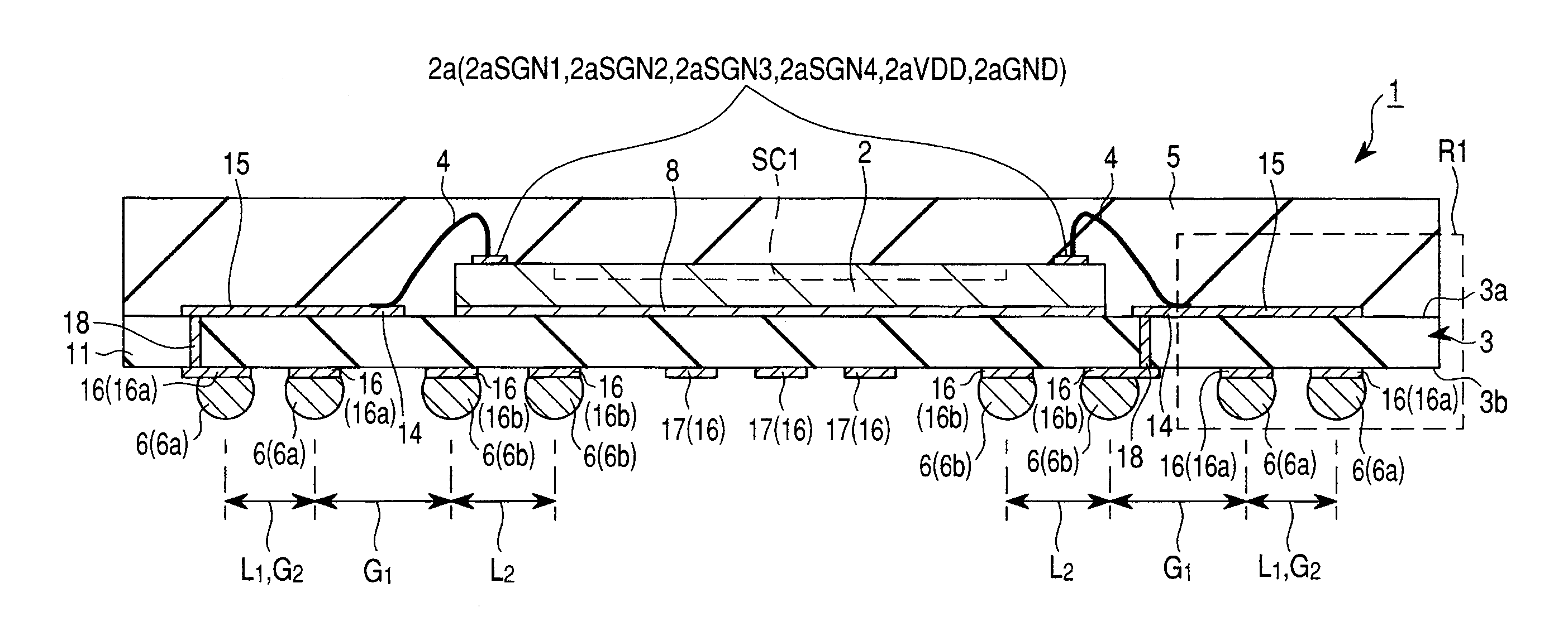
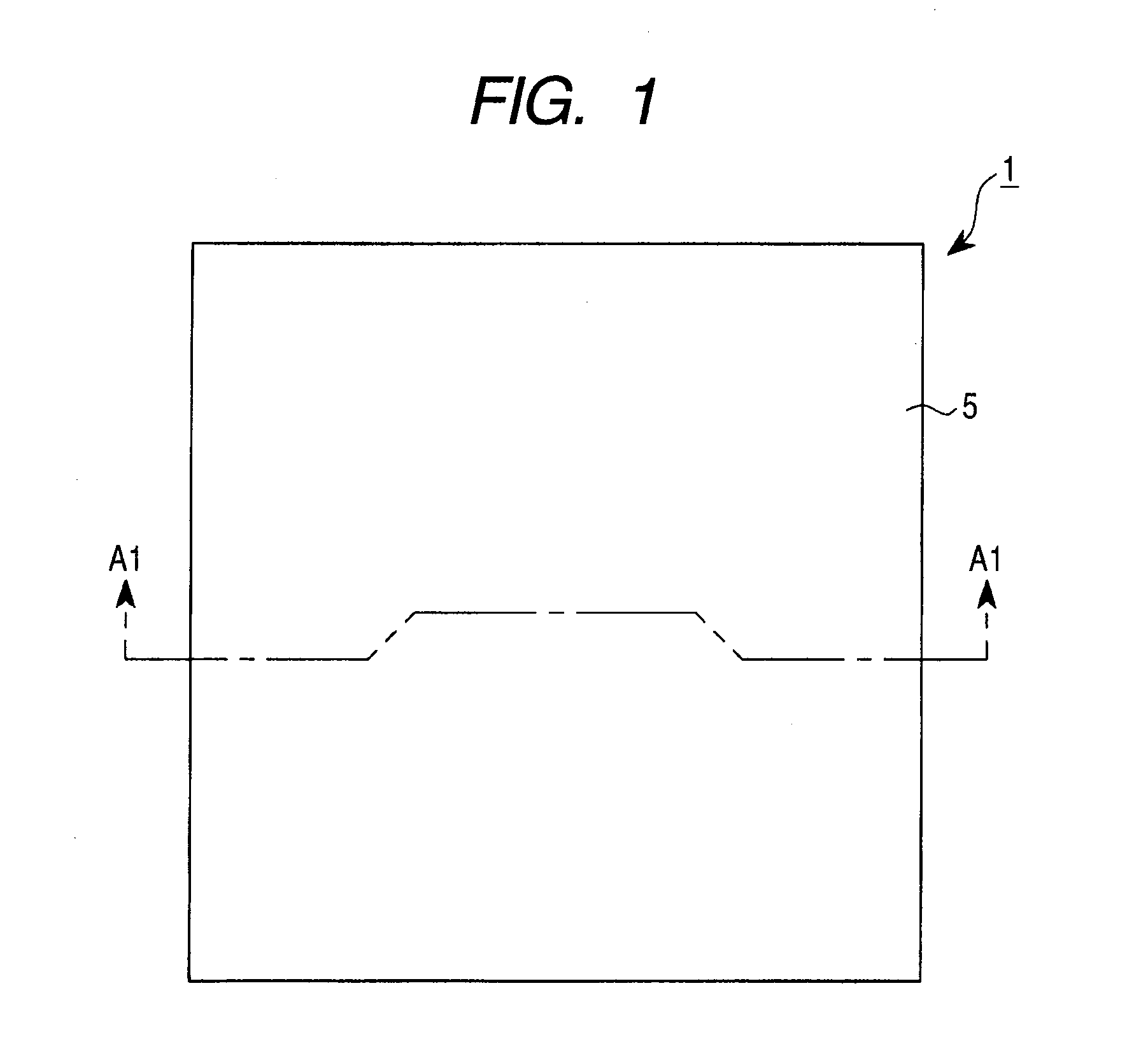
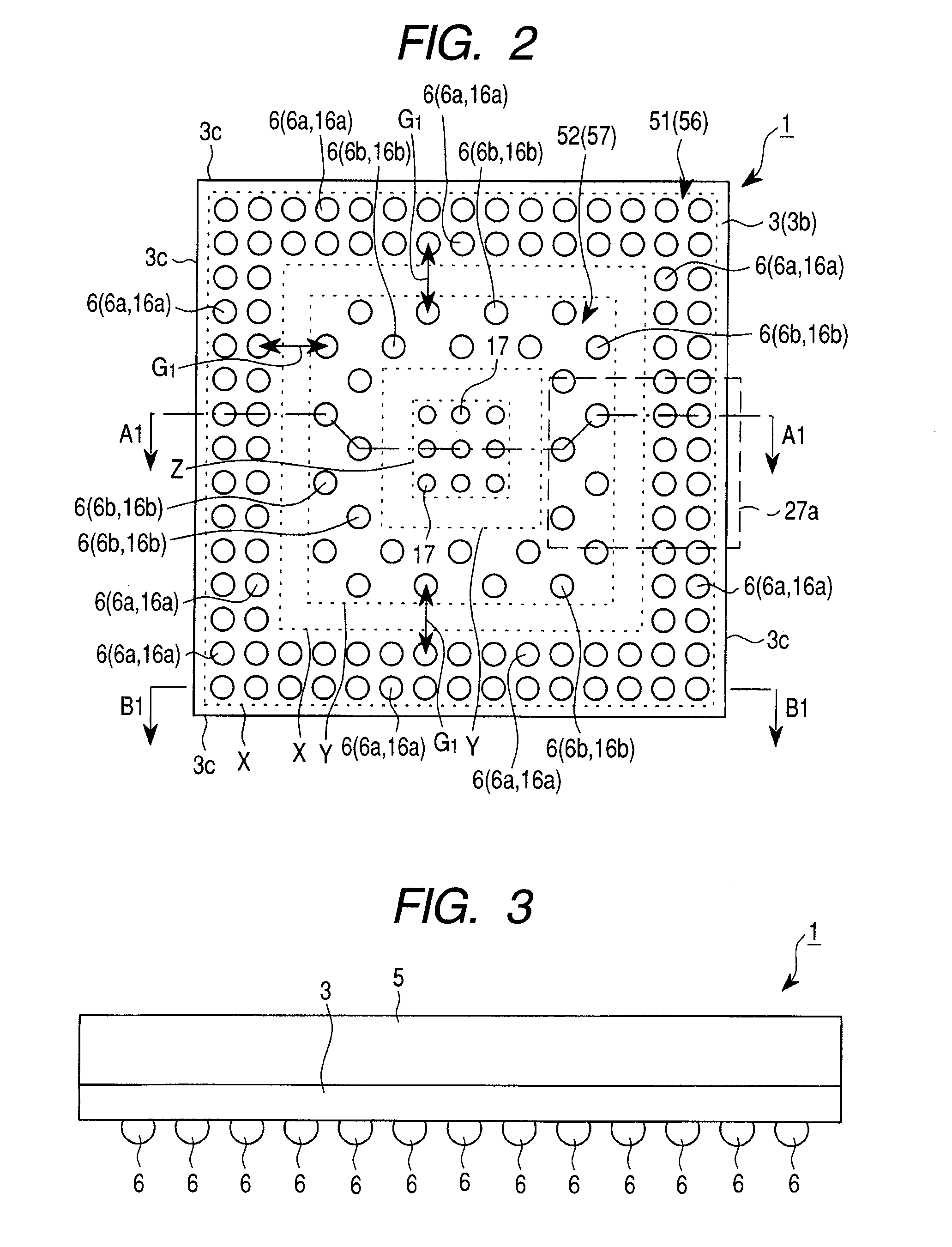
[0095]FIG. 1 is a top view (plan view) of a semiconductor device 1 as an embodiment of the present invention. FIG. 2 is a bottom view (bottom surface view, back surface view, or plan view) of the semiconductor device 1. FIG. 3 is a side view of the semiconductor device 1. FIG. 4 is a cross-sectional view (side cross-sectional view) of the semiconductor device 1. A cross section along the line A1-A1 of each of FIGS. 1 and 2 substantially corresponds to FIG. 4. FIG. 5 is a conceptual plan view (top view) of a semiconductor chip 2 used in the semiconductor device 1. FIG. 6 is a circuit block diagram showing a coupling relationship between the semiconductor chip 2 and external LSIs. FIG. 7 is a conceptual plan perspective view (top view) of the semiconductor device 1 when the semiconductor device 1 is viewed through a mold resin 5.

[0096]The semiconductor device 1 of the present embodi...

embodiment 2

[0217]A semiconductor device of Embodiment 2 of the present invention will be described with reference to the drawings.

[0218]FIG. 43 is a cross-sectional view (side cross-sectional view) of the semiconductor device 1 according to Embodiment 2, which corresponds to FIG. 4 described above.

[0219]In the semiconductor device 1 of FIGS. 1 to 4 described above, the plural terminals for testing 17 are arranged in the vicinity of the center of the lower surface 3b of the wiring substrate 3. However, the present embodiment and Embodiments 3 to 8 shown below are not limited thereto.

[0220]For example, in a case where the number of the solder balls 6 serving as signal supply paths further increases as a semiconductor device becomes higher in functionality, and all the solder balls 6a and 6b in the first solder ball group 51, and in the second solder ball group 52 are used exclusively as the solder balls 6 serving as the signal supply paths, solder balls 6f (or lands 16f for coupling to the solde...

embodiment 3

[0223]A semiconductor device of Embodiment 3 of the present invention will be described with reference to the drawings.

[0224]FIG. 44 is a bottom view (bottom surface view, back surface view, or plan view) of a semiconductor device 1a of the present embodiment, which corresponds to FIG. 2 of Embodiment 1 described above. FIGS. 45 to 48 are illustrative views of the semiconductor device 1a, in which FIG. 45 shows only the solder balls 6 (i.e., solder balls 6c) belonging to a solder ball group 51a at the lower surface 3b of the wiring substrate 3 of the semiconductor device 1a, and corresponds to a plan view in which the depiction of the solder balls 6 belonging to solder ball groups 51a and 52a is omitted. FIG. 46 shows only the solder balls 6 (i.e., solder balls 6d) belonging to the solder ball group 51b at the lower surface 3b of the wiring substrate 3 of the semiconductor device 1a, and corresponds to a plan view in which the depiction of the solder balls 6 belonging to the solder ...


PUM


Abstract

An improvement is achieved in the mounting reliability of a semiconductor device. A semiconductor chip is mounted over an upper surface of a wiring substrate. A plurality of solder balls are disposed individually over a plurality of lands formed on a lower surface of the wiring substrate. The plural lands include a first land group arranged in a plurality of rows and arranged along a peripheral edge portion of the lower surface of the wiring substrate, and a second land group arranged inside the first land group in the lower surface of the wiring substrate. The lands in the first land group are arranged with a first pitch, and the lands in the second land group are arranged with a second pitch higher than the first pitch.

Description

CROSS-REFERENCE TO RELATED APPLICATIONS[0001]The disclosure of Japanese Patent Application No. 2008-262682 filed on Oct. 9, 2008 including the specification, drawings and abstract is incorporated herein by reference in its entirety.BACKGROUND OF THE INVENTION[0002]The present invention relates to a semiconductor device, a manufacturing method thereof, and a manufacturing method of a semiconductor module, and particularly to a technology which is effective when applied to a semiconductor device in which a semiconductor chip is mounted on a wiring substrate, and solder balls are arranged on the lower surface of the wiring substrate, a manufacturing method thereof, and a manufacturing method of a semiconductor module using the semiconductor device.[0003]There are numerous types of package structures of semiconductor devices, such as a ball grid array (BGA) type semiconductor device using a wiring substrate, and a quad flat package (QFP) type semiconductor device using a lead frame. Amo...

Claims


Application Information

Patent Timeline
IPC IPC(8): H01L23/48H01L21/60
CPCH01L23/13H01L23/49838H01L24/02H01L24/16H01L24/17H01L24/45H01L24/48H01L24/49H01L24/97H01L25/0657H01L2223/54486H01L2224/05553H01L2224/16225H01L2224/29339H01L2224/32014H01L2224/32145H01L2224/32225H01L2224/45144H01L2224/48091H01L2224/48227H01L2224/48228H01L2224/4824H01L2224/484H01L2224/48599H01L2224/49175H01L2224/73204H01L2224/73215H01L2224/73265H01L2224/83101H01L2224/83191H01L2224/97H01L2225/0651H01L2225/06517H01L2924/01002H01L2924/01004H01L2924/01005H01L2924/01013H01L2924/01014H01L2924/01029H01L2924/01033H01L2924/01047H01L2924/0105H01L2924/01057H01L2924/01075H01L2924/01078H01L2924/01079H01L2924/01082H01L2924/01083H01L2924/014H01L2924/07802H01L2924/14H01L2924/15184H01L2924/15192H01L2924/15311H01L2924/19041H01L2924/19043H01L2924/19105H01L2924/3511H05K3/3436H05K2201/094H01L24/32H01L2924/01006H01L2924/01019H01L2924/01021H01L2924/0132H01L2924/0133H01L2924/1517H01L2224/29111H01L2224/29139H01L2224/81191H01L2224/131H01L2224/0401H01L2224/06135H01L2924/00014H01L2224/85H01L2224/81H01L2224/83H01L2224/92247H01L2924/00H01L2924/00012H01L2224/13111H01L24/73H01L2224/04042H01L2224/73253H01L2924/10162H01L2924/15183H01L2924/181Y02P70/50H01L2224/85399H01L2224/05599
Inventor HAYASHI, YOSHINARI
Owner RENESAS ELECTRONICS CORP
Why Eureka
Try Eureka