High accuracy beam placement for local area navigation

a local area and beam technology, applied in the direction of semiconductor/solid-state device testing/measurement, image enhancement, instruments, etc., can solve the problems of sample drift in the beam shift navigation system, adversely affecting the performance of the finished semiconductor device, and small margin of error in processing, etc., to achieve high accuracy

Active Publication Date: 2010-04-15
FEI CO
View PDF21 Cites 41 Cited by
  • Summary
  • Abstract
  • Description
  • Claims
  • Application Information

AI Technical Summary

Benefits of technology

[0011]Once the image and the coordinate system have been properly aligned, the alignment can be transferred to the sample itself by way of one or more transfer fiducials. One or more readily identifiable features on the sample in the vicinity of the feature of interest are selected and the offset between the transfer fiducial(s) and the feature of interest is recorded. The sample can then be re-imaged at a much smaller field of view based upon the coordinate system alignment. Once the transfer fiducials are identified in the second image, the recorded offsets can be used to locate the feature of interest and accurately position the particle beam.
[0012]According to preferred embodiments of the present invention, the combination of large area, high resolution scanning, digital zoom and registration of the image to an idealized coordinate system enables navigation around a local area without relying on stage movements. Once the image is acquired any sample or beam drift will not affect the alignment.

Problems solved by technology

As design rules shrink, the margin for error in processing becomes smaller.
Even small deviations from design dimensions may adversely affect the performance of a finished semiconductor device.
Beam shift navigation systems suffer from sample drift, non-linearity in displacement, and are typically limited in field of view.
Without a high accuracy stage (like a laser encoded stage) it is not possible to drive the stage directly to the location of interest with accuracy of 100 nm or less.
Laser stages may have the capability for 100 nm accuracy but are expensive and limit the system flexibility as the stage generally cannot be tilted, thereby losing functionality.

Method used


Image

  • High accuracy beam placement for local area navigation
  • High accuracy beam placement for local area navigation
  • High accuracy beam placement for local area navigation

Examples


Embodiment Construction

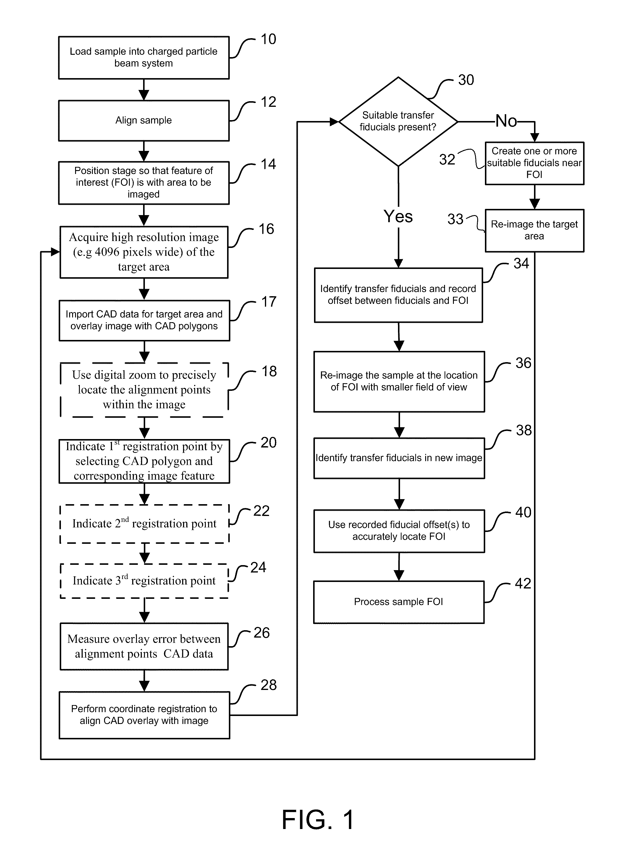
[0028]Preferred embodiments of the present invention are directed at methods for high accuracy beam placement for local area navigation in the field of semiconductor chip manufacturing. This invention demonstrates a method where high accuracy navigation to the site of interest within a relatively large local area (e.g. an area 200 μm×200 μm) is possible even where the stage / navigation system is not normally capable of such high accuracy navigation.

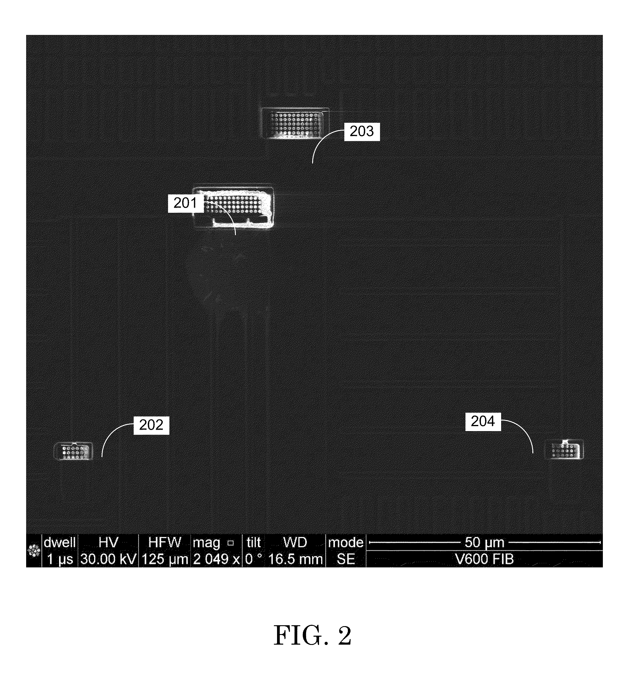
[0029]According to preferred embodiments of the present invention, a high-resolution image of a relatively large target area (a larger area including the location of a feature of interest and one or more suitable alignment marks) is first acquired. For example, a suitably high-resolution area might be 250 μm wide with a resolution approximately 4096 pixels wide. According to one preferred embodiment, the area of interest is overlaid with CAD polygons and a two or three point CAD polygon re-registration is performed. Digital zoom is then ut...


PUM


Abstract

An improved method of high accuracy beam placement for local area navigation in the field of semiconductor chip manufacturing. This invention demonstrates a method where high accuracy navigation to the site of interest within a relatively large local area (e.g. an area 200 μm×200 μm) is possible even where the stage / navigation system is not normally capable of such high accuracy navigation. The combination of large area, high-resolution scanning, digital zoom and registration of the image to an idealized coordinate system enables navigation around a local area without relying on stage movements. Once the image is acquired any sample or beam drift will not affect the alignment. Preferred embodiments thus allow accurate navigation to a site on a sample with sub-100 nm accuracy, even without a high-accuracy stage / navigation system.

Description

[0001]This application claims priority from U.S. Provisional Application No. 61 / 104,732, filed on Oct. 12, 2008, which is hereby incorporated by reference.TECHNICAL FIELD OF THE INVENTION[0002]The present invention relates to stage navigation and beam placement in particle beam systems and, in particular, to high accuracy local area navigation to a site of interest on a sample surface using acquisition of a high resolution image by FIB or SEM means.BACKGROUND OF THE INVENTION[0003]Semiconductor manufacturing, such as the fabrication of integrated circuits, typically entails the use of photolithography. A semiconductor substrate on which circuits are being formed, usually a silicon wafer, is coated with a material, such as a photoresist, that changes solubility when exposed to radiation. A lithography tool, such as a mask or reticle, positioned between the radiation source and the semiconductor substrate casts a shadow to control which areas of the substrate are exposed to the radiat...

Claims


Application Information

Patent Timeline
Patent Type & Authority Applications(United States)
IPC IPC(8): G06K9/00
CPCG06T7/0042G06T2207/10061G06T2207/30148H01J37/222H01J37/28H01L2924/0002H01J2237/31749H01L22/12H01J37/3045H01L2924/00G06T7/73
Inventor YOUNG, RICHARD J.RUE, CHADCARLESON, PETER D.
Owner FEI CO
Why Eureka
Try Eureka