Organic transistor and manufacture method thereof
a technology of organic semiconductors and manufacturing methods, applied in the direction of thermoelectric device junction materials, semiconductor devices, electrical apparatus, etc., can solve the problems of difficult high-resolution patterns, difficult to provide low-molecular organic semiconductor materials, and large pitch of organic tfts, so as to reduce the thickness of the organic semiconductor layer formed, increase the step height, and facilitate contact
- Summary
- Abstract
- Description
- Claims
- Application Information
AI Technical Summary
Benefits of technology
Problems solved by technology
Method used
Image
Examples
example 1
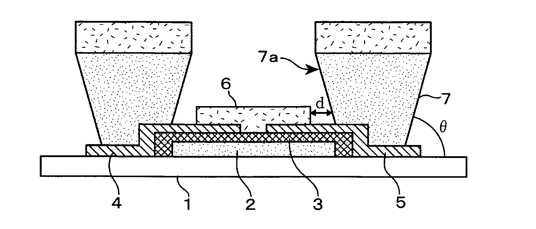
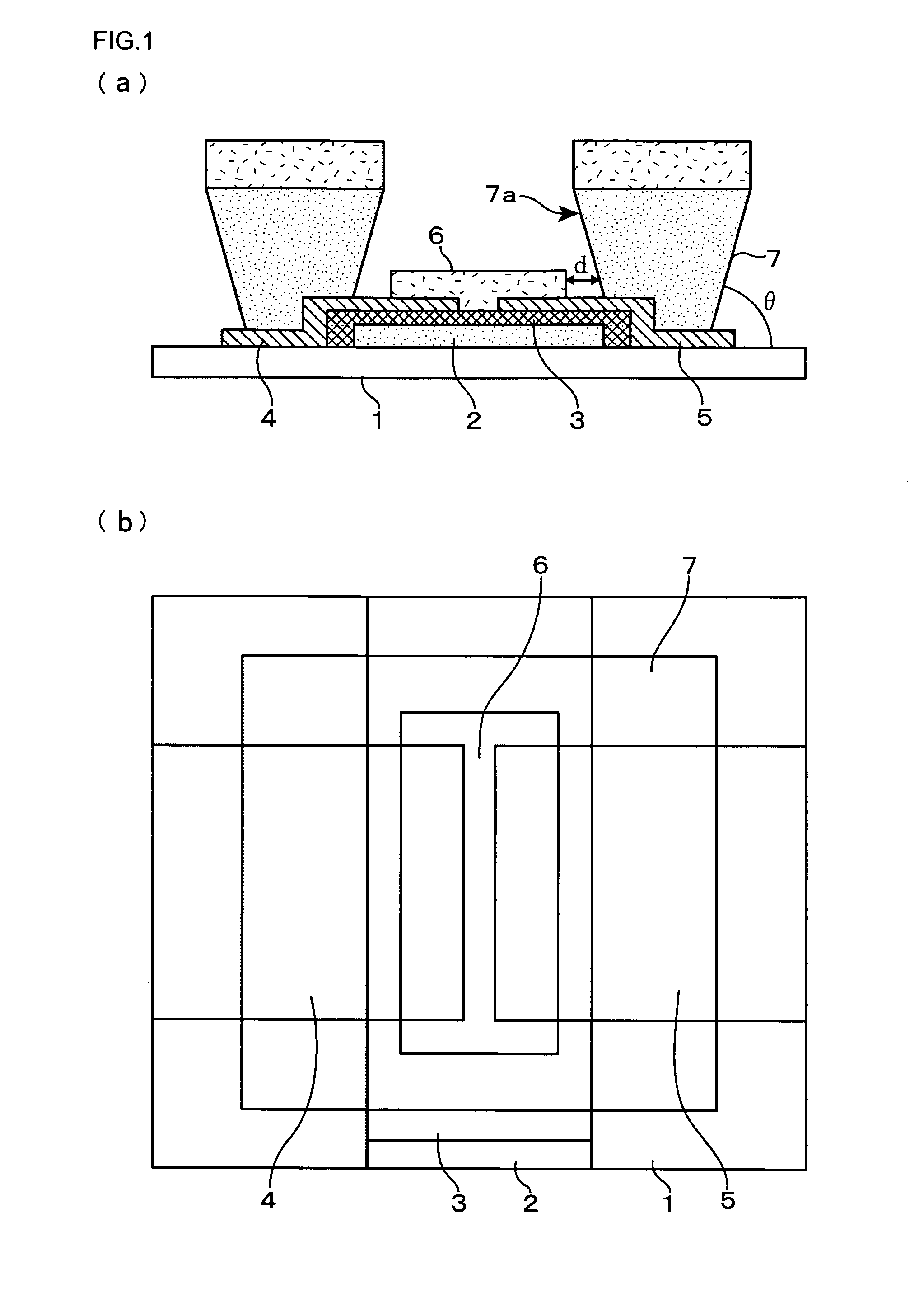
[0065]In Example 1, the organic TFTs of the bottom contact type shown in FIG. 1 were produced and the characteristics thereof were evaluated.
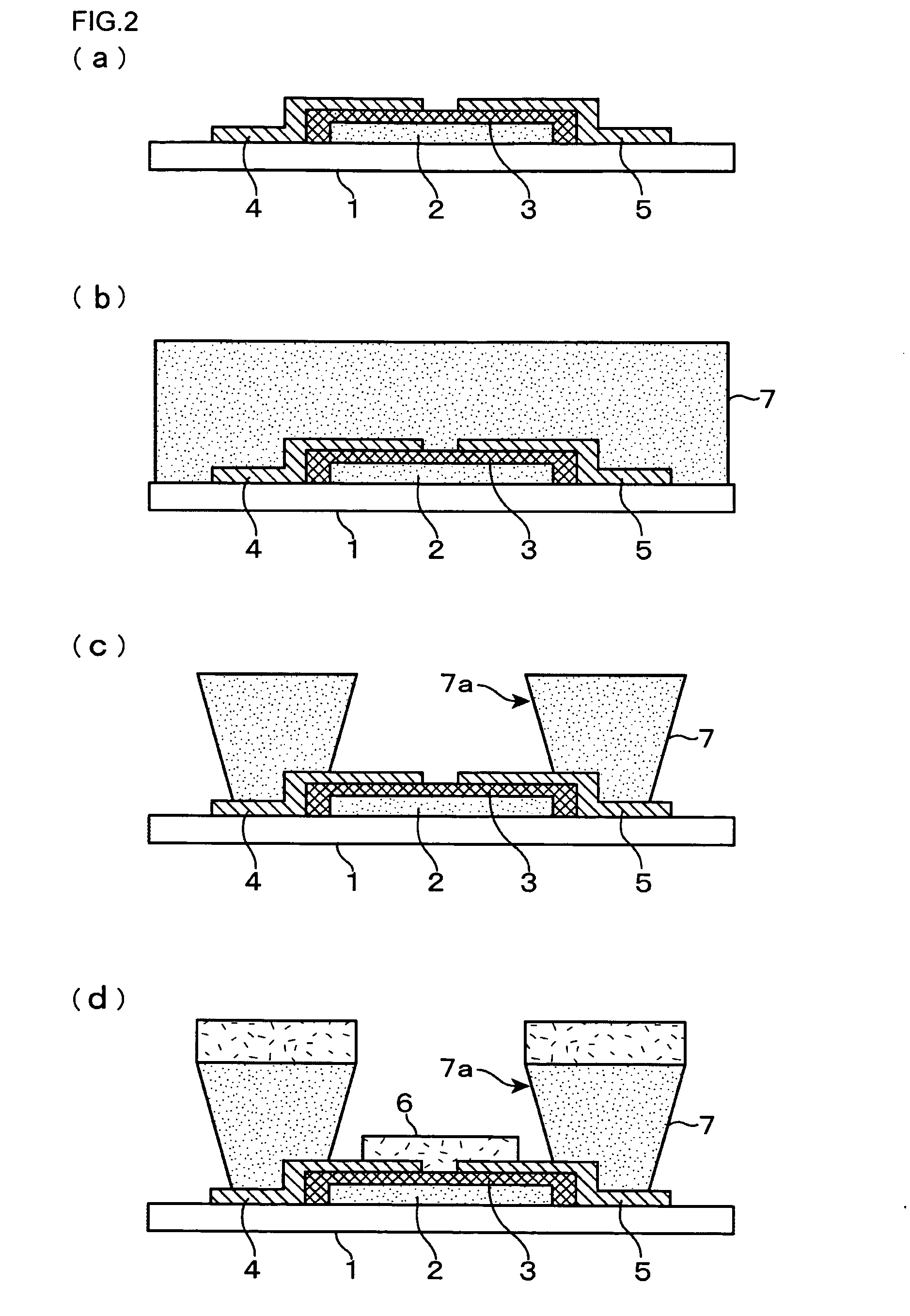
[0066]Each of the organic TFTs had a channel length and a channel width of 5 μm and 400 μm, respectively. A glass substrate was used as the substrate 1, and Ta was deposited thereon and patterned as the gate electrode 2. Ta had a thickness of 200 nm and the patterning was performed with a dry etching method. Next, the gate insulating layer 3 made of Ta2O5 was formed on the surface of Ta with the anodization method to have a thickness of 150 nm. A stacked film of Cr / Au was formed thereon as the source and drain electrodes 4 and 5 to have thicknesses of 5 nm and 100 nm, respectively. The source and drain electrodes 4 and 5 were patterned by using a lift-off method. Next, a photoresist was applied as the insulating layer 7 onto the entire surface over the source and drain electrodes 4 and 5 and was patterned through exposure to form the opening po...
example 2
[0067]In Example 2, the organic light emitting transistors shown in FIG. 3 were produced and the characteristics thereof were evaluated.
[0068]A glass substrate was used as the substrate 1, and an IZO film was deposited on the substrate 1 and patterned as the transparent gate electrode 2. The IZO film had a thickness of 100 nm and the patterning was performed with a wet etching method. Next, a photoresist was formed as the gate insulating layer 3 on the gate electrode 2 to have a thickness of 300 nm. Then, Au was vapor-evaporated as the source electrode 4 to have a thickness of 30 nm. The source electrode 4 was patterned with the wet etching method into the line shape. Next, the insulating layer 7 was patterned to include the opening portion 7a opened to provide the area where the organic functional layer 9 should be formed. A negative photoresist was applied to the entire surface as the insulating layer 7 and was patterned through exposure to provide the opening portion 7 having the...
PUM
 Abstract
Description
Claims
Application Information


