Display driving apparatus

a technology of driving apparatus and display, which is applied in the field of display driving apparatus, can solve the problems of difficult to secure the matching characteristics, long driving time, and difficulty in obtaining matching characteristics, and achieve the effects of reducing power consumption, reducing chip area and driving delay, and reducing the amount of data curren

Inactive Publication Date: 2010-04-22
SILICON WORKS CO LTD
View PDF15 Cites 32 Cited by
  • Summary
  • Abstract
  • Description
  • Claims
  • Application Information

AI Technical Summary

Benefits of technology

[0037]In the display driving apparatus in accordance with the present invention, power consumption, a chip area, and a driving delay may be minimized, and under-damping occurring during driving a high data current may be removed.

Problems solved by technology

However, the current mode driving method has a disadvantage in that the driving time is too long due to large parasitic capacitance existing in a data line and a transistor of the AMOLED panel.
However, the resistance achieved by such a method has a difficulty in obtaining matching characteristics due to properties of process and materials.
Further, the larger the resistance is, the more difficult it is to secure the matching characteristics.
The larger the resistance, the more likely a problem will arise when inter-resistor matching of a data line.
Moreover, since the parasitic capacitance CPP present in the data line changes according to a panel or a location of the panel, it is substantially difficult to design a driving chip considering a deviation of the parasitic capacitance CPP in the capacitor CPC.
This causes the requirement of an additional area and power consumption for embodying the OTA.
Furthermore, because an output impedance of the OTA is large, a low frequency pole is formed by the output impedance of the OTA, namely, gate capacitance of a first transistor M1 and a second transistor M2, thereby resulting in operation instability.
Moreover, since the driving apparatuses shown in FIG. 5 and FIG. 6 use a constant current source IB, the performance is restricted according to the size of the constant current source IB in a charging or discharging procedure of the parasitic capacitances CPc, CDP present in the data line.
This also leads to an increase in power consumption of the driving apparatus.

Method used


Image

  • Display driving apparatus
  • Display driving apparatus
  • Display driving apparatus

Examples


first embodiment

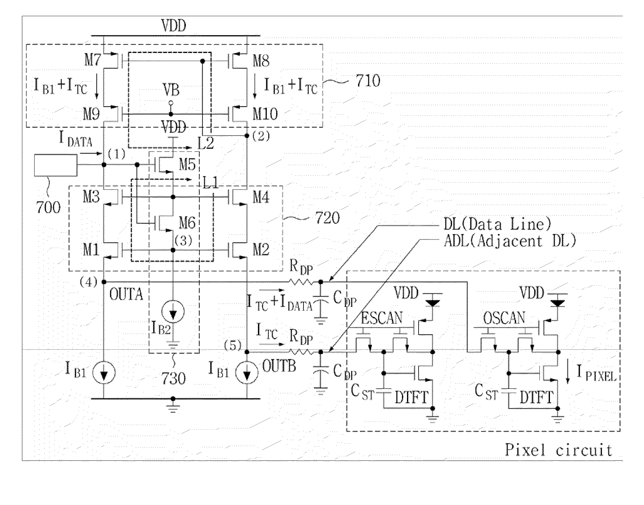
[0051]FIG. 7 is a circuitry diagram illustrating a display driving apparatus in accordance with a first embodiment of the present invention.

[0052]Referring to FIG. 7, the display driving apparatus in accordance with the first embodiment of the present invention includes a current digital / analog converter (DAC) 700, a data line DL, an adjacent data line ADL, a current mirror 710, a current output unit 720, a source follower 730, and a constant current source IB1.

[0053]The current DAC 700 generates a data current corresponding to the input of digital data.

[0054]The data line DL is connected to a pixel circuit requiring data writing located on a matrix array of a display panel.

[0055]The adjacent data line ADL is located adjacent to the data line DL. The adjacent data line ADL has the same parasitic capacitance CDP as that of the data line DL.

[0056]The current mirror 710 may have a stack mirror structure. The current mirror 710 may feedback an excessive charging current ITC generating ...

second embodiment

[0083]Hereinafter, a display driving apparatus in accordance with a second exemplary embodiment of the present invention will be explained with reference to the accompanying drawings.

[0084]FIG. 8 is a circuitry diagram illustrating a display driving apparatus in accordance with a second embodiment of the present invention.

[0085]Referring to FIG. 8, the display driving apparatus in accordance with a second embodiment of the present invention includes a current DAC 800, a data line DL, an adjacent data line ADL, a current mirror 810, a current output unit 820, a first differential amplifier 830, a constant current source IB, dynamic current sources ISINK1 and ISINK2, and a sink current control unit 840.

[0086]The current DAC 800 generates a data current corresponding to an input of digital data.

[0087]The data line DL is connected to a pixel circuit requiring data writing on a matrix array of a display panel.

[0088]The adjacent data line ADL is located adjacent to the data line DL. The a...

third embodiment

[0111]Hereinafter, a display driving apparatus in accordance with a third exemplary embodiment of the present invention will be explained with reference to the accompanying drawings.

[0112]FIG. 11 is illustrates a concept of a loop gain control in accordance with an embodiment of the present invention.

[0113]In a case where a signal path is formed from a node X to a node Y, if a gain block AV between the node X and the node Y forms a negative feedback loop, a gain obtained in the node Y is 1 / (1+AV) less than an original gain.

[0114]FIG. 12 and FIG. 13 are circuit diagrams illustrating display driving apparatuses in accordance with a third embodiment of the present invention to which the concept of a loop gain control is applied.

[0115]Referring to FIG. 12, the display driving apparatus in accordance with the third embodiment of the present invention includes a current DAC 800, a data line DL, an adjacent data line ADL, a current mirror 810, a current output unit 820, a first differentia...


PUM


Abstract

Disclosed is a display driving apparatus. The display driving apparatus comprises: a current DAC generating a data current; a data line connected to a pixel circuit requiring data writing on a matrix array of a display panel; an adjacent data line located adjacent to the data line; a current mirror feedbacking an excessive charging current generating due to parasitic capacitance of the adjacent data line as a charging current for charging parasitic capacitance of the data line; a current output unit connected to the current mirror and including a first driving transistor unit for driving the data line, and a second driving transistor unit for driving the adjacent data line; a source follower driving the current output unit according to an output node voltage of the current DAC; and a first constant current source discharging parasitic capacitance excessively charged in the data line and the adjacent data line.

Description

CROSS-REFERENCE TO RELATED APPLICATION[0001]This application claims priority to Korean Patent Application No. 10-2008-0101424, filed Oct. 16, 2008, the entirety of which is hereby incorporated by reference.BACKGROUND OF THE INVENTION[0002]1. Field of the Invention[0003]The present invention relates to a display driving apparatus.[0004]2. Description of the Related Art[0005]A current mode driving method may prevent spatial non-uniformity and time characteristic change of a thin film transistor forming a backplane of an active-matrix organic light-emitting diode (AMOLED) panel and enable an exact data current to flow to an OLED.[0006]However, the current mode driving method has a disadvantage in that the driving time is too long due to large parasitic capacitance existing in a data line and a transistor of the AMOLED panel. There have been proposed various methods to improve a driving speed while maintaining driving precision of a data current as in the current mode driving method.[00...

Claims


Application Information

Patent Timeline
Patent Type & Authority Applications(United States)
IPC IPC(8): G09G5/00
CPCG09G3/325G09G3/3283G09G2320/0295G09G2310/027G09G2320/0223G09G2300/0842H01L2924/13091H01L2924/14253
Inventor CHO, GYU-HYEONGJEON, YONG-JOONJEON, JIN-YONGJUNG, SEUNG-CHULKIM, KI-DUKLEE, SUNG-WOO
Owner SILICON WORKS CO LTD
Why Eureka
Try Eureka