Manufacturing method of silicon single crystal

a single crystal, silicon technology, applied in the direction of crystal growth process polycrystalline material growth, etc., can solve the problem of difficult to make temperature gradient between solid-liquid interface of silicon single crystal and interior of quartz crucible, and the relationship between intensity of magnetic flux density in molten silicon or its intensity distribution is extremely difficult at present to clarify the relationship between intensity of magnetic flux density and molten silicon intensity, so as to reduce the surface temperature of molten silicon.

Inactive Publication Date: 2010-04-29
COVALENT MATERIALS CORP
View PDF6 Cites 21 Cited by
  • Summary
  • Abstract
  • Description
  • Claims
  • Application Information

AI Technical Summary

Benefits of technology

[0013]Although the MCZ method is superior to the CZ method in controlling concentration of oxygen due to the suppression of the convection flow of the molten silicon, it is difficult to make temperature gradient between solid-liquid interface of silicon single crystal and interior of a quartz crucible. Furthermore, whe...

Problems solved by technology

However, technical investigations from the standpoints of flow control and temperature control of the molten silicon in a quartz crucible are few.
The reason is that it is extremely difficult at present to clarify the relationship among intensity of magnetic flux density in molten silicon or its intensity distribution, the melt flow and temperature distribution based on accurate actual measurement.
Although the MCZ method is superior to the CZ method in controlling concentration of oxygen due to the suppression of the convection flow of the molten silicon, it is difficult to make temperature gradient between...

Method used


Image

  • Manufacturing method of silicon single crystal
  • Manufacturing method of silicon single crystal
  • Manufacturing method of silicon single crystal

Examples


first exemplary embodiment

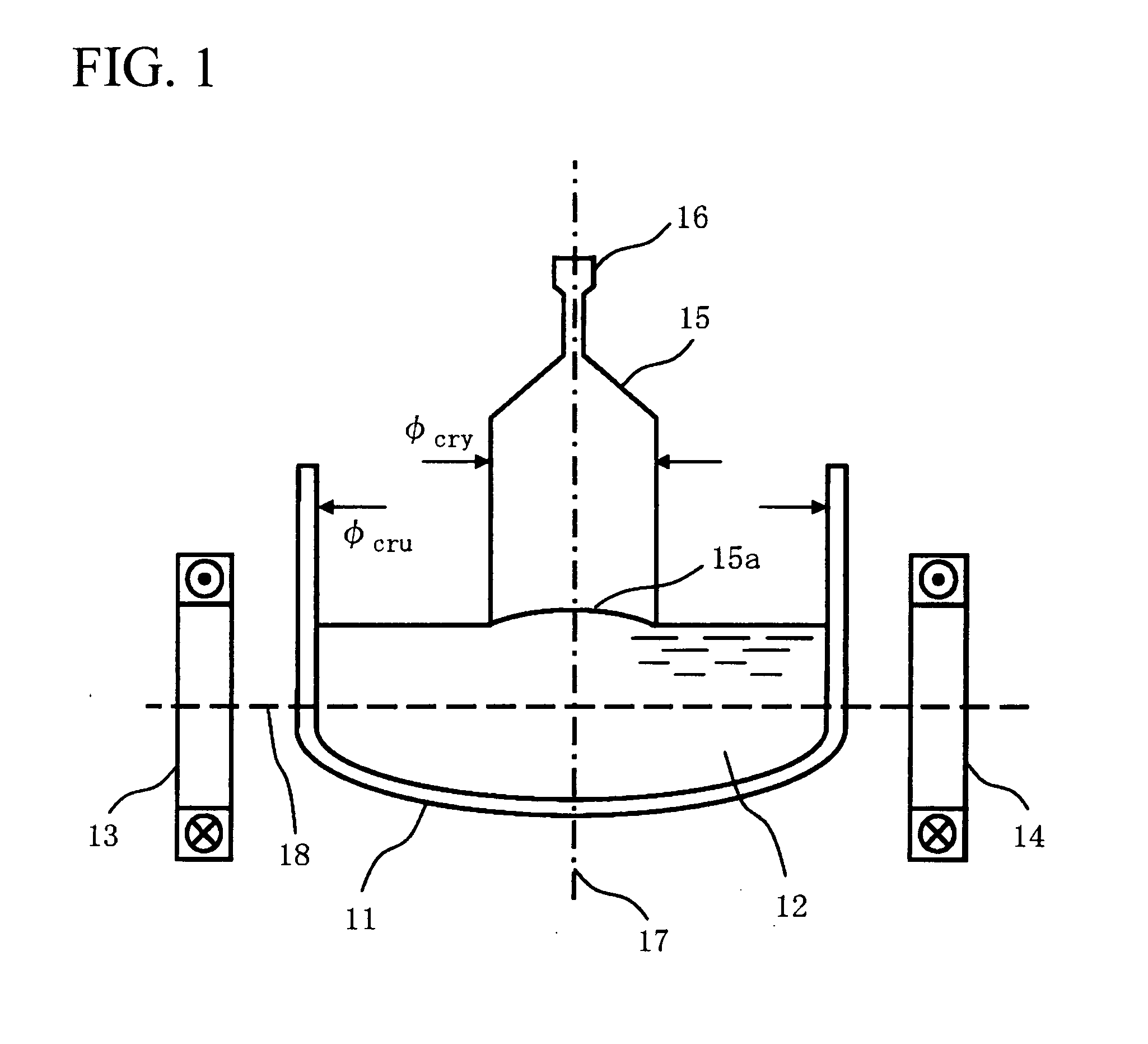
[0049]An optimization method of horizontal magnetic field in pulling out silicon single crystal according to a first exemplary embodiment of the present invention is described below.

[0050]In the growth of silicon single crystal, a molten silicon 12 is stored in a bottomed cylindrical quartz crucible 11, and transverse magnetic field (referred to “horizontal magnetic field”) is applied to the molten silicon 12 from a pair of exciting coils 13 and 14 arranged sides portions of the quartz crucible 11 so as to face each other. Silicon crystal 15 is pulled up and grown in the order of a neck part in a so-called dash-necking process using a seed crystal 16 as a nucleus, a shoulder part increasing a diameter to the desired crystal diameter, a straight body part having a constant diameter and a tail part which decreases a diameter.

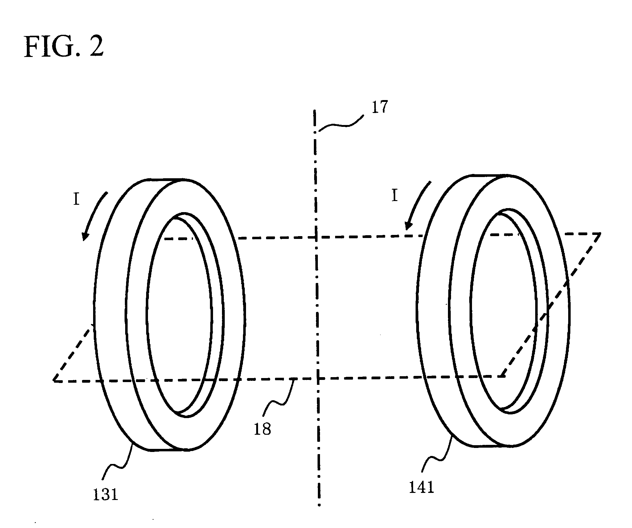
[0051]The exciting coils 13 and 14 are a pair of circular exciting coils 131 and 141 having the same shape and size arranged so as to face with each other as show...

second exemplary embodiment

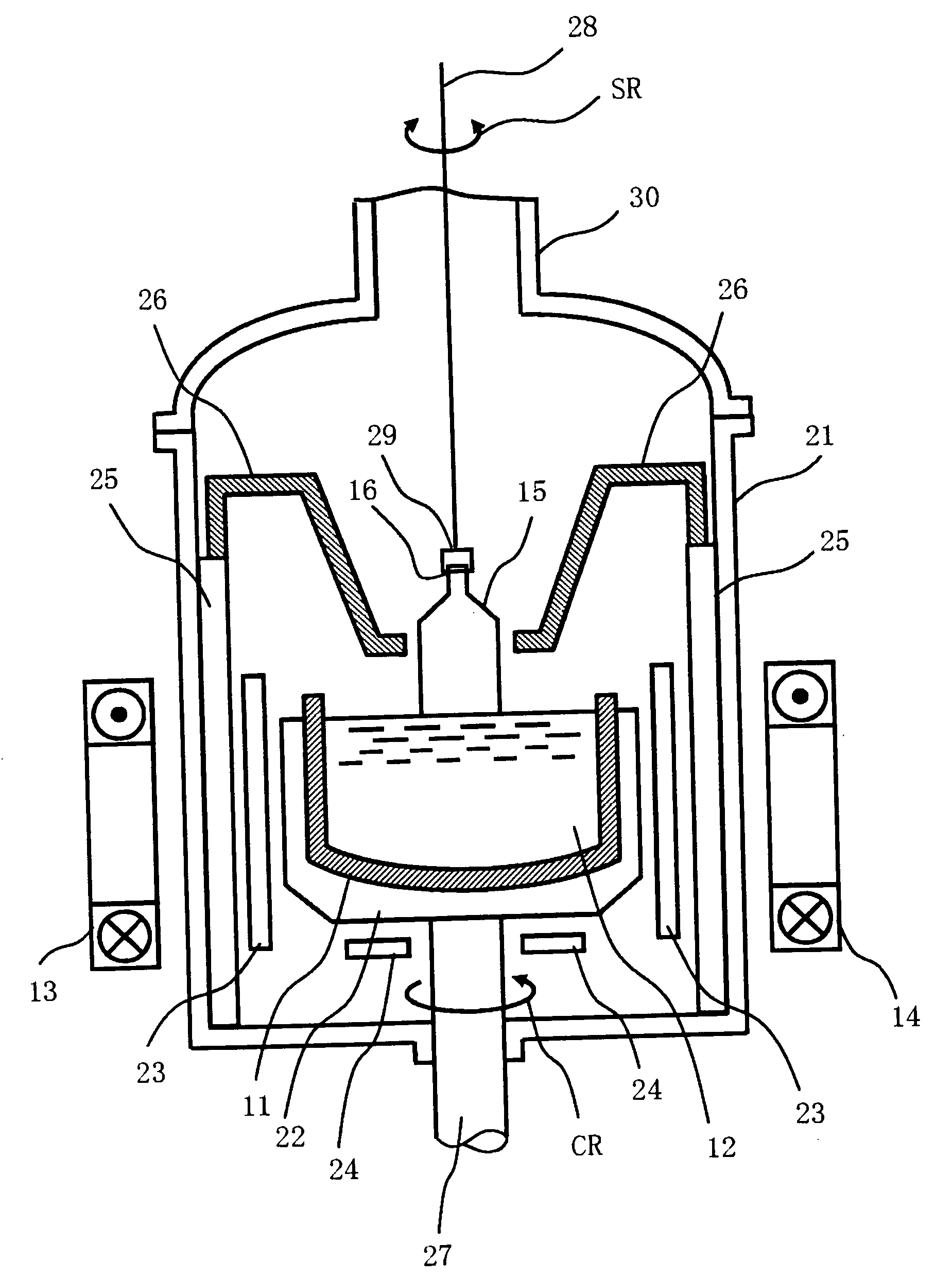
[0103]A manufacturing method of silicon single crystal according to a second exemplary embodiment of the present invention is described below by referring to FIG. 14.

[0104]The manufacturing apparatus of silicon single crystal has a bottomed cylindrical main chamber 21. In the main chamber 21, a quartz crucible 11 adapted to filled with molten silicon 12 and a graphite crucible 22 arranged on outside of the quartz crucible 11 are provided in a form of a double structure. Further, the manufacturing apparatus has side heaters 23 and bottom heaters 24 for heating the graphite crucible 22 with a given distance to the graphite crucible 22. Further, heat-insulting members 25 are arranged at a position outside the side heaters 23 and the bottom heaters 24 and between those heaters and the main chamber 21. Furthermore, radiant shields 26 having, for example, a cut conical shape, for shielding heat of radiation from the side heaters 23 to silicon single crystal 15 is arranged at the upper edg...


PUM


Abstract

In appropriate setting of magnetic field applied to a molten silicon 12 stored in a cylindrical quartz crucible 11, the maximum value B0 of magnetic flux density on a vertical symmetric axis 17 as a cylindrical axis of the quartz crucible 11 in horizontal magnetic field generated by a pair of exciting coils 13 and 14 calls B0. On circle at which horizontally symmetric plane 18 traversing and perpendicular to a vertically symmetric axis 17 becoming magnetic flux B0 crosses an inner diameter of the quartz crucible 11, the minimum value of magnetic flux density calls Bmin, and the maximum value of magnetic flux density calls Bmax. Those magnetic flux densities B0, Bmin and Bmax are adjusted to be given ranges, and upward flow and temperature of a molten silicon 12 at the lower part of a solid-liquid interface 15a are appropriately controlled.

Description

BACKGROUND OF THE INVENTION[0001]1. Field of the Invention[0002]The present invention relates to a silicon single crystal growth technique by MCZ method (Magnetic field applied CZochralski method). More particularly, the present invention relates to a manufacturing method of silicon single crystal having a large diameter, such as 300 mm or more.[0003]2. Description of Related Art[0004]Many silicon single crystals used as a silicon wafer in a substrate of a semiconductor device are grown by a pulling out method so-called a CZ method. Currently, a silicon single crystal ingot grown by this method has a diameter of about 300 mm (12 inches), and further increasing the diameter (for example, 450 mm (18 inches)) is investigated.[0005]In the CZ method, a cylindrical quartz crucible with bottom placed in a growth furnace is filled with raw material silicon (generally polycrystal silicon), and the silicon is heated with a heater to form molten silicon. Seed crystal is attached to the surface...

Claims


Application Information

Patent Timeline
IPC IPC(8): C30B15/22
CPCC30B29/06C30B15/305C30B15/22
Inventor FU, SENLINHISAICHI, TOSHIO
Owner COVALENT MATERIALS CORP
Why Eureka
Try Eureka