Compound for photoresist, photoresist liquid, and etching method using the same

a technology of photoresist and liquid, applied in the field of compound for photoresist, photoresist liquid, and etching method using the same, can solve the problems of reducing light-emitting efficiency, difficult to consistently achieve a surface of uniform roughness, and variation in product performan

Inactive Publication Date: 2010-04-29
FUJIFILM CORP
View PDF13 Cites 5 Cited by
  • Summary
  • Abstract
  • Description
  • Claims
  • Application Information

AI Technical Summary

Benefits of technology

[0009]Accordingly, it is an object of the present invention to provide a novel compound for photoresist, employed for minute processing by means ...

Problems solved by technology

Since the refractive index of the uppermost layer (or outermost layer) of the light outlet of the chip differs from that of the resin of the package, reflection occurs at the boundary between the two, diminishing light-emitting efficiency.
However, the former method requires an onerous process of fabricating a mold, as w...

Method used


Image

  • Compound for photoresist, photoresist liquid, and etching method using the same
  • Compound for photoresist, photoresist liquid, and etching method using the same
  • Compound for photoresist, photoresist liquid, and etching method using the same

Examples


example 1

Formation of Photoresist Film

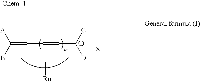
[0208]A 2 g quantity of oxonol dye (Example Compound (II)-5, film λmax: 378 nm; thermal decomposition temperature: 216° C.) was dissolved in 100 mL of tetrafluoropropanol (TFP), and spin coated on a disk-shaped silicon substrate (0.6 mm in thickness, 120 mm in outer diameter, 15 mm in inner diameter) to form a coating film. The spin coating was conducted by dispensing a coating liquid on the inner circumferential portion of the substrate at a coating starting rotational speed of 500 rpm and a coating ending rotational speed of 100 rpm. The rotational speed was gradually increased to 2,200 rpm to dry the coating film. The coating film that was formed was 100 nm in thickness.

[0209]The silicon substrate on which the coating film had been formed was placed in a NEO500 made by Pulstec Industrial Co., Ltd. (wavelength: 405 nm, NA: 0.65), and a laser beam was directed onto the surface of the coating film. The laser beam irradiation conditions were as set forth ...

example 2

Formation of Irregularities

[0213]The silicon substrate processed in Example 1 was subjected to RIE etching under the following conditions from the surface side on which the coating film had been formed, after which the coating film was removed with ethanol as stripping solution. The formation of minute irregularities on the surface of the silicon substrate from which the coating film had been removed was visually confirmed. From this result, it can be understood that the coating film processed in Example 1 had functioned as an etching mask.

[0214]Etching gas: SF6+CHF3 (1:1)

[0215]Etching depth: 50 nm

examples 3 to 14

[0216]With the exception that Example Compounds given in Table 2 below were employed as oxonol dyes, pits were formed on the coating film at a 0.5 micrometer pitch in the same manner as in Example 1 by irradiation of the coating film surface with a laser beam in the same manner as in Example 1.

TABLE 3ThermalExampledecompositionCompoundλmax of film (nm)temperature (° C.)Example 3(II-1)380188Example 4(II-2)393245Example 5(II-3)385183Example 6(II-4)378200Example 7(II-16)382228Example 8(II-17)393265Example 9(II-18)385166Example 10(II-19)378220Example 11(II-20)378200Example 12(II-21)377145Example 13(II-22)462188Example 14(II-23)572237


PUM


Abstract

The present invention relates to a compound for photoresist, selected from the group consisting of a compound comprising an oxonol dye skeleton, a cyanine dye, a styryl dye, a compound comprising a merocyanine dye skeleton, a compound comprising a phthalocyanine dye skeleton, an azo compound, and a complex compound of an azo compound and a metal ion. The present invention further provides a photoresist liquid comprising at least one of the compound for photoresist and a method of etching a surface being processed using the photoresist liquid.

Description

CROSS-REFERENCE TO RELATED APPLICATIONS[0001]This application claims the benefit of priority to Japanese Patent Application Nos. 2007-054289 filed on Mar. 5, 2007, 2007-196756 filed on Jul. 27, 2007, 2007-212149 filed on Aug. 16, 2007, 2007-267664 filed on Oct. 15, 2007, 2007-267665 filed on Oct. 15, 2007, 2008-047243 filed on Feb. 28, 2008, 2008-047127 filed on Feb. 28, 2008, 2008-047130 filed on Feb. 28, 2008, 2008-047237 filed on Feb. 28, 2008, and 2008-047238 filed on Feb. 28, 2008, which are expressly incorporated herein by reference in their entirety.TECHNICAL FIELD[0002]The present invention relates to a compound for photoresist and a photoresist liquid, that permits the formation of minute patterns. The present invention further relates to a method of etching a surface being processed using the photoresist liquid.BACKGROUND TECHNIQUE[0003]In the process of manufacturing electronic components such as semiconductor elements, magnetic bubble memories, and integrated circuits, t...

Claims


Application Information

Patent Timeline
IPC IPC(8): G03F7/00C07D277/04C07D215/12C07D213/57C09B47/04C09B29/036
CPCC09B23/0091C09B23/04C09B23/06C09B23/083C09B23/102C09B23/107C09B29/0037C09B29/004C09B29/0048C09B29/0066C09B29/0088C09B29/0092C09B29/0803C09B29/083C09B29/12C09B29/26C09B29/325C09B29/337C09B29/338C09B29/3604C09B29/3608C09B29/3634C09B29/3652C09B29/366C09B29/3673C09B47/14C09B47/18C09B47/26C09B69/06G03F7/091C09B23/0008C09B23/0016C09B23/005C09B23/0066C09B23/086C09B29/0033C09B29/0081C09B29/081C09B47/20C09B47/22C09B47/24C09B69/04G03F7/36C09B45/20C09B47/12G03F7/0045
Inventor WATANABE, TETSUYA
Owner FUJIFILM CORP
Why Eureka
Try Eureka