Misalignment compensation for proximity communication

a technology of proximity communication and misalignment compensation, which is applied in the field of semiconductor chips, can solve the problems of reducing the effectiveness of face-to-face proximity communication, difficult and expensive implementation, and art has failed to teach a graceful degrading of link performance, so as to improve the performance of the proximity communication system, increase or decrease the misalignment

Active Publication Date: 2010-05-06
ORACLE INT CORP
View PDF13 Cites 8 Cited by
  • Summary
  • Abstract
  • Description
  • Claims
  • Application Information

AI Technical Summary

Benefits of technology

[0009]In some embodiments, the signal level of the transmitted signal is increased with increasing misalignment.
[0013]In one embodiment based on reduced data rate, the increased bit period is used to increase the offset compensation of the receiver. The offset compensation may include a resistive drain or a pre-charging of the receiver amplifier.
[0016]In still another embodiment, one or more neighboring channel is turned off to reduce cross talk arising from misalignment.
[0017]In some embodiments, the data granularity is increased for loss of signal strength.
[0018]In one embodiment of variable granularity involving pulse width modulation (PWM), the number of signal bits determining the width of a PWM is reduced. Alternatively, the width of the PWM period is increased, thereby reducing the data rate.
[0020]In some embodiments of control of the degradation combinable with different embodiment of the types of control, a circuit dynamically detects increased or decreased misalignment between the proximity communication chips and accordingly degrades or improves performance of the proximity communication system.

Problems solved by technology

Any misalignment between chips will reduce the effectiveness of face-to-face proximity communication, whether that communication is moderated through capacitive coupling, inductive coupling, optical coupling, or a direct conductive path.
Although such actuators may be effective in some situations to correct misalignment, they are often difficult and expensive to implement.
However, the prior art has failed to teach a method of gracefully degrading the link performance in response to chip misalignment without necessarily realigning the chips.
This degradation may take the form of slowing down the data rate of the channel, increasing the latency in the channel, or increasing the power used by the channel.

Method used


Image

  • Misalignment compensation for proximity communication
  • Misalignment compensation for proximity communication
  • Misalignment compensation for proximity communication

Examples


Embodiment Construction

[0033]The following description is presented to enable any person skilled in the art to make and use the invention and is provided in the context of a particular application and its requirements. Various modifications to the disclosed embodiments will be readily apparent to those skilled in the art, and the general principles defined herein may be applied to other embodiments and applications without departing from the spirit and scope of the present invention. Thus, the present invention is not limited to the embodiments shown but is to be accorded the widest scope consistent with the principles and features disclosed herein.

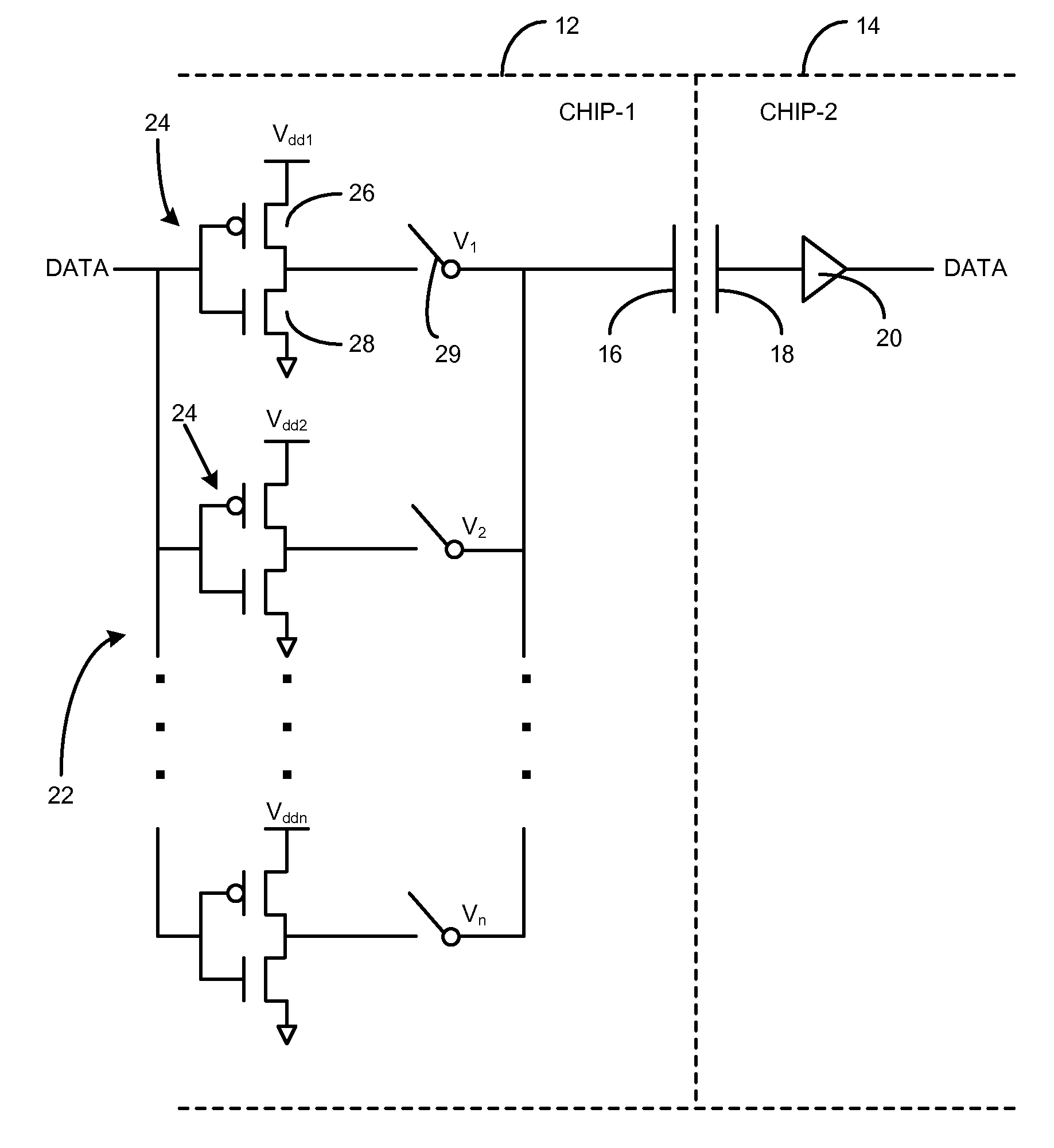
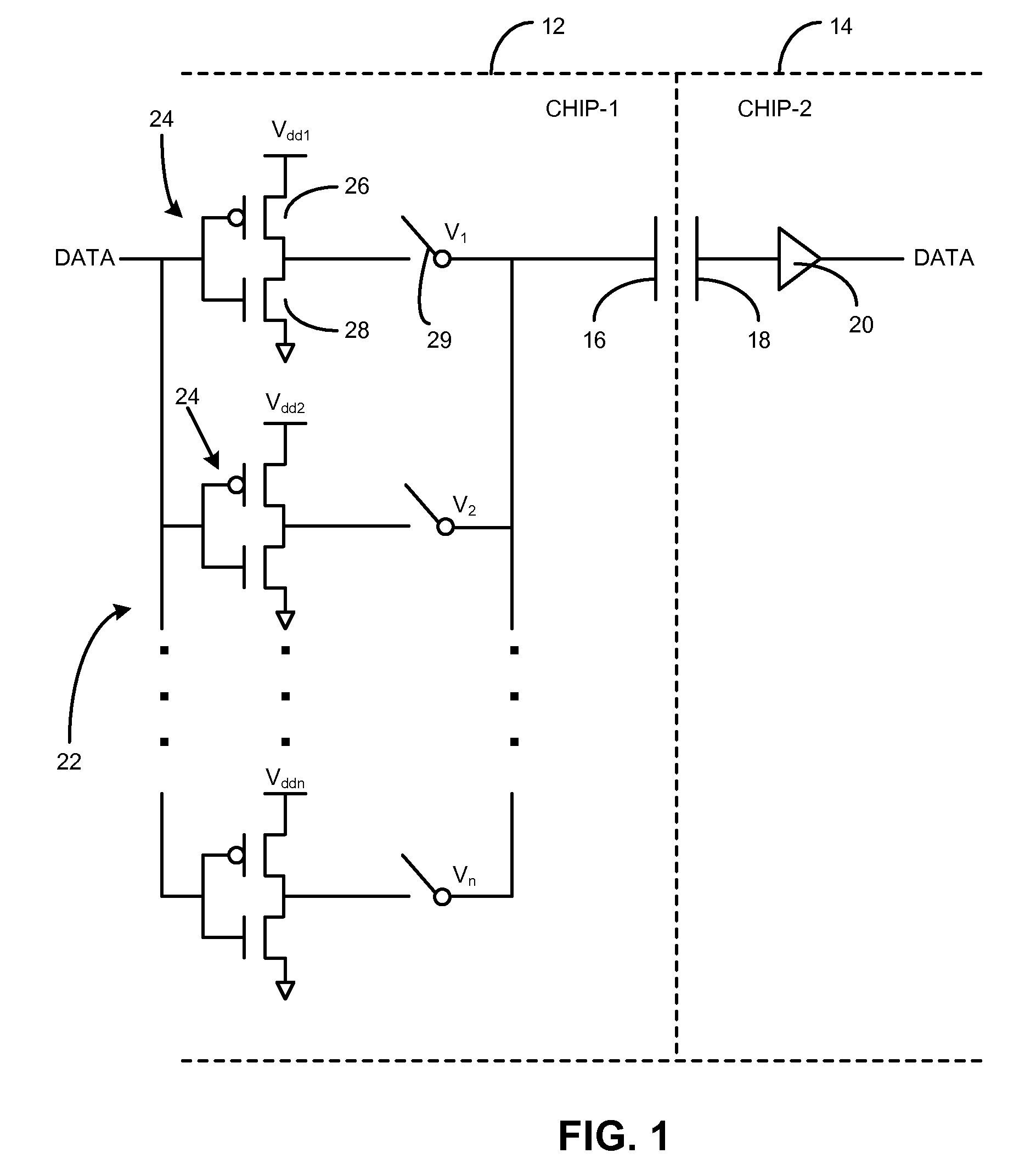
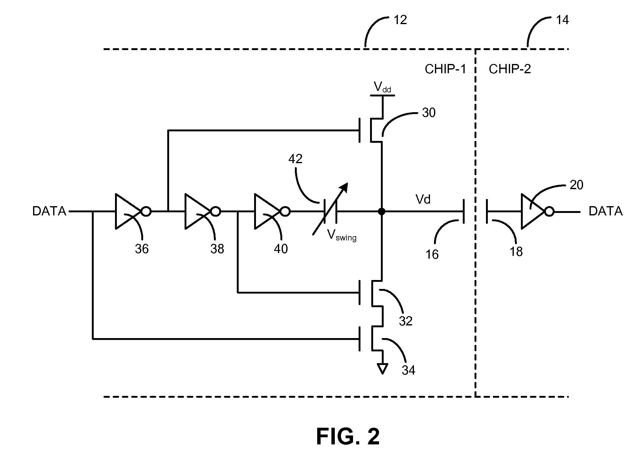
[0034]A proximity communication channel between two chips requires the two chips to be accurately aligned face-to-face. Data can then be sent between the chips using either capacitive, inductive, conductive, or optical coupling means. Any chip misalignment will reduce the coupling between the two chips and lower the effectiveness of the communication. This misa...


PUM

PropertyMeasurementUnit
signal currentaaaaaaaaaa
lengthaaaaaaaaaa
sizeaaaaaaaaaa

Abstract

In a proximity communication system, transmit elements on one chip are aligned with receive elements on a second chip juxtaposed with the first chip. However, if the elements are misaligned, either statically or dynamically, the coupling between chips is degraded. The misalignment may be compensated by controllably degrading performance of the system. For example, the transmit signal strength may be increased. The bit period or the time period for biasing each bit may be increased, thereby decreasing the bandwidth. Multiple coupling elements, such as capacitors, may be ganged together, thereby decreasing the number of channels. The granularity of symbols, such as images, may be increased by decreasing the number of bits per symbol. Multiple coupling elements, such as capacitors, may be ganged together, thereby decreasing the number of channels.

Description

BACKGROUND[0001]1. Field of the Invention[0002]This present invention relates to semiconductor chips and their alignment and fixing to another chip or substrate. The invention relates specifically to a method and apparatus for gracefully degrading performance of a proximity communication channel in response to misalignment of one or more semiconductor chips.[0003]2. Related Art[0004]Proximity communication (PxC) is a well known technology that enables communication between two integrated circuit chips, but that also relies upon face-to-face alignment of those chips, as has been explained by Drost et al. in “Proximity Communication,”IEEE Journal of Solid-State Circuits, vol. 39, no. 9, September 2004, pp. 1529-1535. Misalignment between these two chips between which the proximity communication channel is formed may occur for a number of reasons, including but not limited to: inaccurate placement in a package or on a printed circuit board (PCB) or other carrier substrate; temperature ...

Claims


Application Information

Patent Timeline
Patent Type & Authority Applications(United States)
IPC IPC(8): G06K5/04G06F11/00
CPCH01L25/065H04B5/0075H04L1/0009H01L2924/0002H01L2924/00H04B17/318Y10T29/49133
Inventor HO, RONALDKRISHNAMOORTHY, ASHOK V.CUNNINGHAM, JOHN E.DROST, ROBERT J.
Owner ORACLE INT CORP
Why Eureka
Try Eureka