Plasma and thermal anneal treatment to improve oxidation resistance of metal-containing films

a metal-containing film and thermal anneal treatment technology, which is applied in the direction of coatings, chemistry apparatuses and processes, other domestic articles, etc., can solve the problems of lacked accessible or tunable electronic properties of materials used for gate electrodes, dielectric layers to become conductive, and tantalum materials only being scarcely used for metal gate electrode formation

Inactive Publication Date: 2010-05-13
APPLIED MATERIALS INC
View PDF13 Cites 62 Cited by
  • Summary
  • Abstract
  • Description
  • Claims
  • Application Information

AI Technical Summary

Benefits of technology

[0013]In another embodiment, a method is provided for forming a structure including positioning a substrate in a processing chamber, and the substrate comprising a silicon substrate surface, depositing a high k dielectric material on a silicon substrate surface, depositing a tantalum nitride layer on high k dielectric material, treating a deposited tantalum nitride layer with a thermal anneal, a plasma, anneal, or both, depositing a polysilicon layer on the treated tantalum nitride layer, depositing a patterned hard mark layer on the polysilicon layer, selectively etching the polysilicon lay

Problems solved by technology

However, the materials used for gate electrodes have lacked accessible or tunable electronic properties by varying the compositions of the contained materials.
While tantalum materials have been used as barrier layers, tantalum materials have only been scarcely used for the formation of metal gate electrodes, despite the variety of electronic characteristics available from tantalum materials.
Formation of tantalum-containing barrier layers, such as tantalum, tantalum nitride, and other tantalum materials, in multi-level integrated circuits poses many challenges to process control, particularly with respect to contact formation

Method used


Image

  • Plasma and thermal anneal treatment to improve oxidation resistance of metal-containing films
  • Plasma and thermal anneal treatment to improve oxidation resistance of metal-containing films
  • Plasma and thermal anneal treatment to improve oxidation resistance of metal-containing films

Examples


example 1

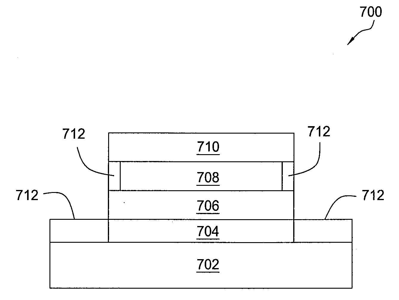
[0091]Metal Nitride film densification. An atomic layer deposited tantalum nitride layer from an organometallic tantalum precursor and ammonia precursor was observed to have a deposition thickness of 80 Å. The deposited tantalum nitride layer may be deposited by any atomic layer process including process described herein or as described in U.S. Pat. No. 7,211,508, issued on May 1, 2007, which is incorporated by reference to the extent not inconsistent with the disclosure and claim aspects herein.

[0092]The deposited ALD tantalum nitride layer was exposed to a thermal anneal at 800° C. and 1000° C. while supplying nitrogen gas to the processing chamber at a flow rate of about 10000, sccm, heating the substrate for a period of 30 seconds, and maintaining a chamber pressure of about 100 Torr. The anneal layer was observed to have a thickness of about 65 Å at 800° C. and a thickness of about 59 Å at 1000° C. The tantalum atomic percentage for the deposited layer was observed to be about ...


PUM

PropertyMeasurementUnit
Temperatureaaaaaaaaaa

Abstract

Method and apparatus are provided for treatment of a deposited material layer. In one embodiment, a method is provided for processing a substrate including depositing a metal-containing layer using an atomic layer deposition technique, exposing the metal-containing layer to a plasma treatment process at a temperature of less than about 200° C., and exposing the metal-containing layer to a thermal anneal process at a temperature of about 600° C. or greater. The plasma treatment process and/or the thermal anneal process may use a nitrating gas, which may form a passivating surface or layer with the metal-containing layer.

Description

BACKGROUND OF THE INVENTION[0001]1. Field of the Invention[0002]Embodiments of the present invention relate to a method for manufacturing integrated circuit devices. More particularly, embodiments of the invention relate to a system and process for depositing and treating an atomic layer deposition material layer in a semiconductor device.[0003]2. Description of the Related Art[0004]The electronic device industry and the semiconductor industry continue to strive for larger production yields while increasing the uniformity of layers deposited on substrates having increasingly larger surface areas. These same factors in combination with new materials also provide higher integration of circuits per unit area on the substrate. As circuit integration increases, the need for greater uniformity and process control regarding layer characteristics rises.[0005]Several areas of fabrication that are constantly improving include the formation of metal gate electrodes and the deposition of contac...

Claims


Application Information

Patent Timeline
IPC IPC(8): H01L21/321
CPCB32B38/0008H01L29/66181B32B2038/0092B32B2309/02B32B2309/04B32B2309/105B32B2319/00B32B2457/00C23C16/56H01L21/28061H01L21/28247H01L21/28562H01L21/76843H01L21/76856H01L21/76862H01L21/76864H01L27/10861H01L27/10888H01L29/4941H01L29/4966B32B38/0036H10B12/038H10B12/485
Inventor TJANDRA, AGUS SOFIANYOKOTA, YOSHITAKAOLSEN, CHRISTOPHER S.
Owner APPLIED MATERIALS INC
Why Eureka
Try Eureka