Solid-state imaging device, method for producing same, and camera

a solid-state imaging and camera technology, applied in the direction of radio-controlled devices, television system scanning details, television systems, etc., can solve the problems of reducing sensitivity, difficult to form and the method of forming the p-type semiconductor region by ion implantation and annealing with activation at a high temperature for a long period of time is not desirable, so as to suppress the generation of dark curren

Active Publication Date: 2010-06-10
SONY CORP
View PDF6 Cites 35 Cited by
  • Summary
  • Abstract
  • Description
  • Claims
  • Application Information

AI Technical Summary

Benefits of technology

[0014]According to the embodiments of the present invention, the control gate can control the potential of the photodetector in the vicinity of the first surface, thus suppressing the generation of the dark current. Furthermore, the signal charge is accumulated in the first region of the first conductivity type and in the vicinity of the first surface of the photodetector, thus improving the ability of the transfer gate to read the signal charge.
[0021]According to the embodiments of the present invention, the transparent conductive film can control the potential of the light-receiving surface of the photodetector, thus suppressing the generation of the dark current. Furthermore, since the thickness of the insulating film disposed between the light-receiving surface and the transparent conductive film is set at 50 nm or less, a combination of the insulating film and the transparent conductive film forms an antireflective film. Alternatively, in the case of the stacked insulating film, the thickness of the silicon oxide sub-film in contact with the light-receiving surface is set at 50 nm or less, a combination of the insulating film and the transparent conductive film forms an antireflective film. The resulting antireflective film improves the absorption coefficient of light in the photodetector, thus increasing sensitivity.
[0024]According to the embodiments of the present invention, the film is disposed on the light-receiving surface of the photodetector and has the negative fixed charge, thereby forming a hole accumulation state on the surface of the photodetector and suppressing the generation of the dark current due to the interface state.

Problems solved by technology

Thus, in a low-temperature process at a temperature of 400° C. or lower, it is difficult to form the p-type semiconductor region by ion implantation.
Furthermore, in view of the inhibition of diffusion of impurities, the method for forming the p-type semiconductor region by ion implantation and annealing with activation at a high temperature for a long period of time is not desirable.
In CMOS image sensors, the leads on the pixels disadvantageously blocks light, thus reducing sensitivity.
However, ion implantation limits the formation of the shallow p-type semiconductor region having high-impurity concentration.
The deep p-type semiconductor region may degrade the read ability of the transfer gate because the pn junction of the photodiode is remote from the transfer gate.

Method used


Image

  • Solid-state imaging device, method for producing same, and camera
  • Solid-state imaging device, method for producing same, and camera
  • Solid-state imaging device, method for producing same, and camera

Examples


first embodiment

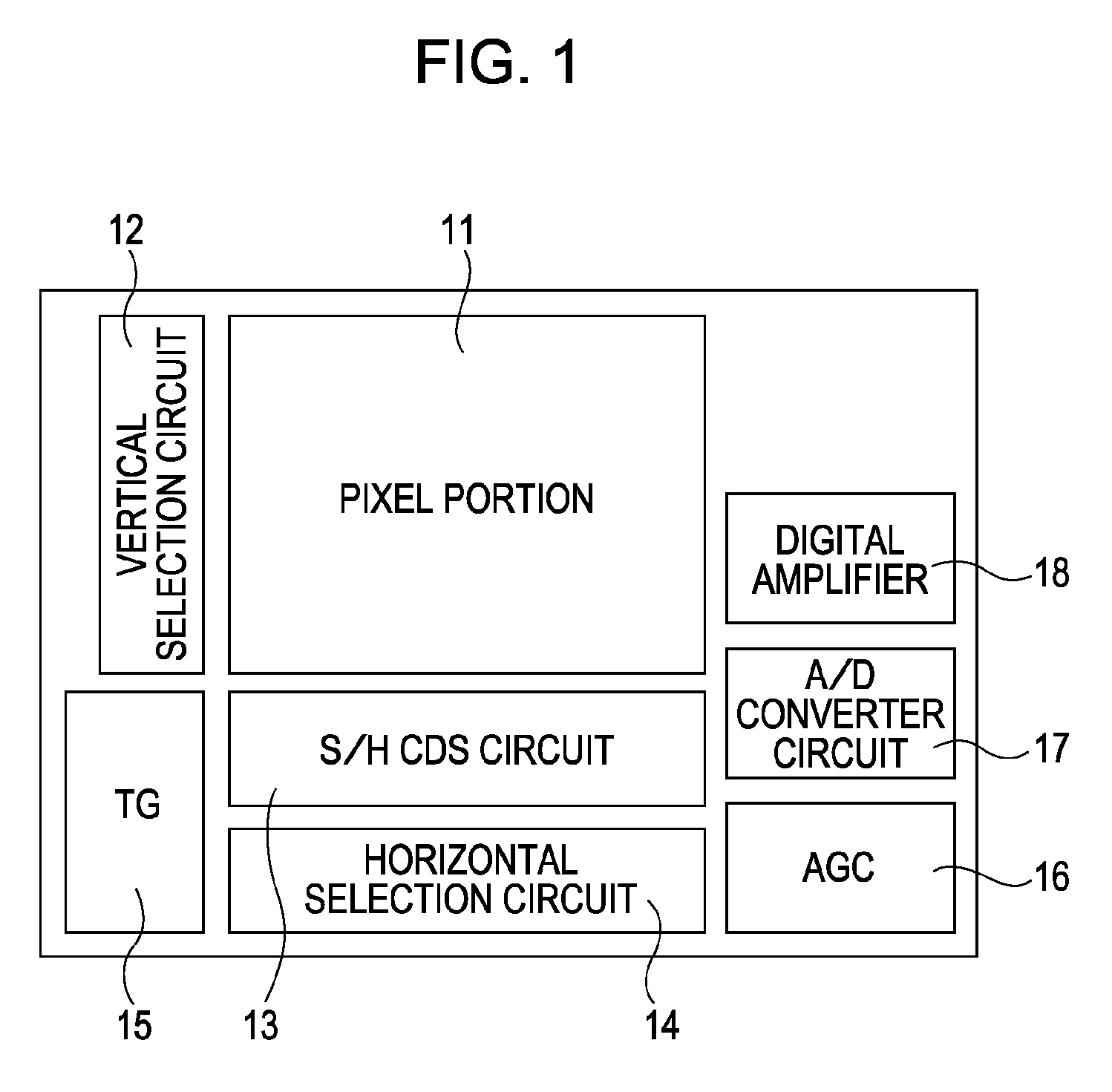
[0058]FIG. 1 is a schematic block diagram of a solid-state imaging device according to an embodiment of the present invention.

[0059]The solid-state imaging device includes a pixel portion 11 and peripheral circuitry, the pixel portion 11 and the peripheral circuitry being disposed on the same semiconductor substrate. In this embodiment, the peripheral circuitry includes a vertical selection circuit 12, a sample-and-hold correlated double sampling (S / H CDS) circuit 13, a horizontal selection circuit 14, a timing generator (TG) 15, an automatic gain control (AGC) circuit 16, an A / D converter circuit 17, and a digital amplifier 18.

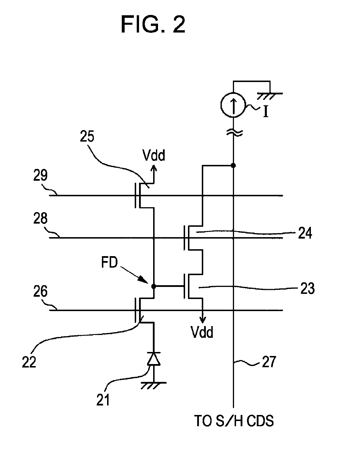
[0060]The pixel portion 11 includes many unit pixels that are arrayed in a matrix, as described below. Address lines and the like extend along rows of the pixels. Signal lines and the like extend along columns of the pixels.

[0061]The vertical selection circuit 12 successively selects the pixels on a row-by-row basis. The vertical selection circuit 12 reads pi...

second embodiment

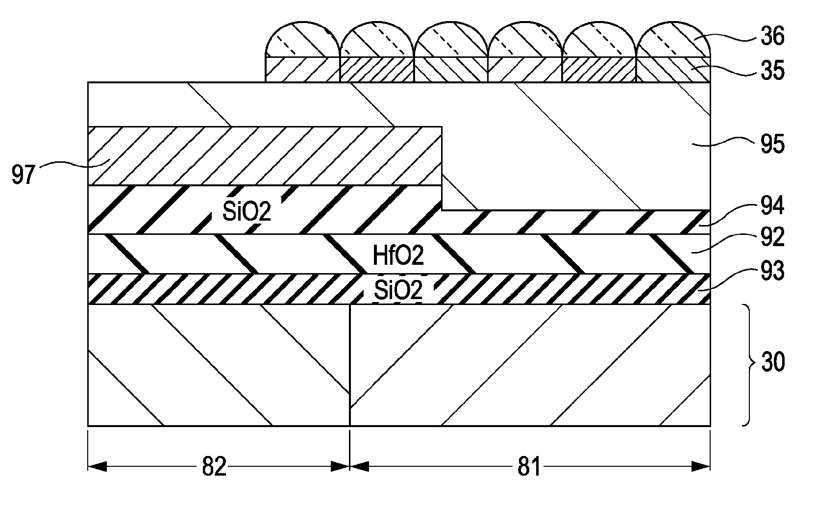
[0119]FIG. 11 is a fragmentary cross-sectional view of the pixel portion of the substrate 30 of a solid-state imaging device according to a second embodiment. The same elements as those in the first embodiment are designated using the same reference numerals, and redundant description is not repeated.

[0120]Two control gates, i.e., a first control gate 52-1 and a second control gate 52-2, are formed on the first surface of the substrate 30 with a gate-insulating film (not shown) provided therebetween. The first control gate 52-1 is located between the transfer gate 51 and the second control gate 52-2. The first and second control gates 52-1 and 52-2 are superposed on the photodetector 31. The first and second control gates 52-1 and 52-2 are composed of, for example, polysilicon. Each of the first and second control gates 52-1 and 52-2 preferably has a thickness comparable to the thickness of the transfer gate 51 in view of processability and resistance. Light is incident on the secon...

third embodiment

[0134]FIG. 13 is a fragmentary cross-sectional view of the pixel portion of the substrate 30 of a solid-state imaging device according to a third embodiment. The same elements as those in the first embodiment are designated using the same reference numerals, and redundant description is not repeated.

[0135]The control gate 52 is formed on the first surface of the substrate 30 with a gate-insulating film (not shown) provided therebetween. In this embodiment, the control gate 52 partially overlaps the photodetector 31. The hole-accumulation region 44 is not formed under the control gate 52. That is, a region where only the control gate 52 is located next to the transfer gate 51 and a region where only the hole-accumulation region 44 is located are formed. Alternatively, the hole-accumulation region 44 may be formed on the entire surface of the photodetector 31. Furthermore, the control gate 52 and the hole-accumulation region 44 may be inversely arranged.

[0136]The above-described solid...


PUM


Abstract

A solid-state imaging device includes a substrate having a first surface and a second surface, light being incident on the second surface side; a wiring layer disposed on the first surface side; a photodetector formed in the substrate and including a first region of a first conductivity type; a transfer gate disposed on the first surface of the substrate and adjacent to the photodetector, the transfer gate transferring a signal charge accumulated in the photodetector; and at least one control gate disposed on the first surface of the substrate and superposed on the photodetector, the control gate controlling the potential of the photodetector in the vicinity of the first surface.

Description

RELATED APPLICATION DATA[0001]This application is a division of U.S. patent application Ser. No. 11 / 677,645, filed Feb. 22, 2007, the entirety of which is incorporated herein by reference to the extent permitted by law. The present application claims the benefit of priority to Japanese Patent Application JP 2006-048173 filed in the Japanese Patent Office on Feb. 24, 2006, and Japanese Patent Application JP 2007-025807 filed in the Japanese Patent Office on Feb. 5, 2007, the entireties both of which are incorporated by reference herein to the extent permitted by law.BACKGROUND OF THE INVENTION[0002]1. Field of the Invention[0003]The present invention relates to a solid-state imaging device, a method for producing the device, and a camera including the solid-state imaging device.[0004]2. Description of the Related Art[0005]It is known that in solid-state imaging devices, such as charge-coupled device (CCD) image sensors and complementary metal oxide semiconductor (CMOS) image sensors,...

Claims


Application Information

Patent Timeline
Patent Type & Authority Applications(United States)
IPC IPC(8): H04N5/335H01L27/148H01L31/18H01L27/14H01L27/146H04N5/361H04N5/369H04N5/374
CPCH01L27/14609H01L27/14643H01L27/1464H01L31/022466H01L27/14685H01L31/022475H04N25/63
Inventor MARUYAMA, YASUSHIYAMAGUCHI, TETSUJIANDO, TAKASHIHIYAMA, SUSUMUOHGISHI, YUKO
Owner SONY CORP
Why Eureka
Try Eureka