Semiconductor device and method of manufacturing same

a semiconductor and device technology, applied in semiconductor devices, digital storage, instruments, etc., can solve the problem of low drive current, achieve the effect of suppressing the reduction of drive current, increasing the absolute value of threshold voltage, and increasing the impurity concentration of the channel region

Active Publication Date: 2010-07-01
RENESAS ELECTRONICS CORP
View PDF7 Cites 10 Cited by
  • Summary
  • Abstract
  • Description
  • Claims
  • Application Information

AI Technical Summary

Benefits of technology

[0014]According to a semiconductor device and a method of manufacturing the same in an embodiment of the present invention, the sum of the concentration of lanthanum atom and the concentration of magnesium atom in the second nMIS high-k film is lower than the sum of the concentration of lanthanum atom and the concentration of magnesium atom in the first nMIS high-k film. Consequently, it is possible to increase the absolute value of threshold voltage of the second nMIS transistor having the second nMIS high-k film compared to the absolute value of threshold voltage of the first nMIS transistor having the first nMIS high-k film without the need to increase the impurity concentration of the channel region. Consequently, it is possible to suppress the reduction of the drive current of the second nMIS transistor while increasing the absolute value of threshold voltage of the second nMIS transistor compared to the absolute value of threshold voltage of the first nMIS transistor.
[0015]According to a semiconductor device and a method of manufacturing the same in another embodiment of the present invention, the concentration of aluminum atom in the second pMIS high-k film is lower than the concentration of aluminum atom in the first pMIS high-k film. Consequently, it is possible to increase the absolute value of threshold voltage of the second pMIS transistor having the second pMIS high-k film compared to the absolute value of threshold voltage of the first pMIS transistor having the first pMIS high-k film without the need to increase the impurity concentration of the channel region. Consequently, it is possible to suppress the reduction of the drive current of the second pMIS transistor while increasing the absolute value of threshold voltage of the second pMIS transistor compared to the absolute value of threshold voltage of the first pMIS transistor.

Problems solved by technology

Consequently, there is a problem that among the MIS transistors, the one with the greater absolute value of threshold voltage has a low drive current.

Method used


Image

  • Semiconductor device and method of manufacturing same
  • Semiconductor device and method of manufacturing same
  • Semiconductor device and method of manufacturing same

Examples


first embodiment

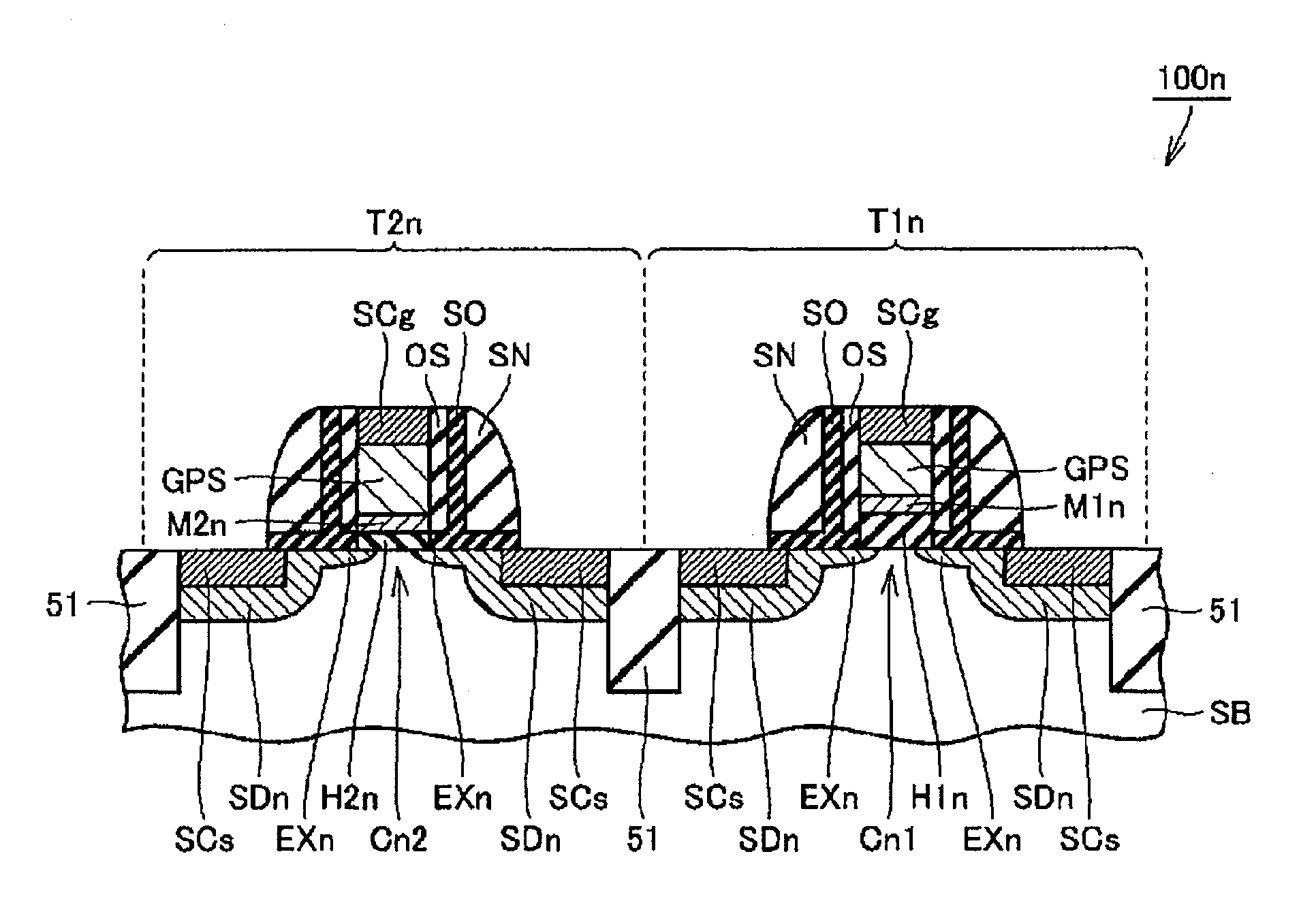
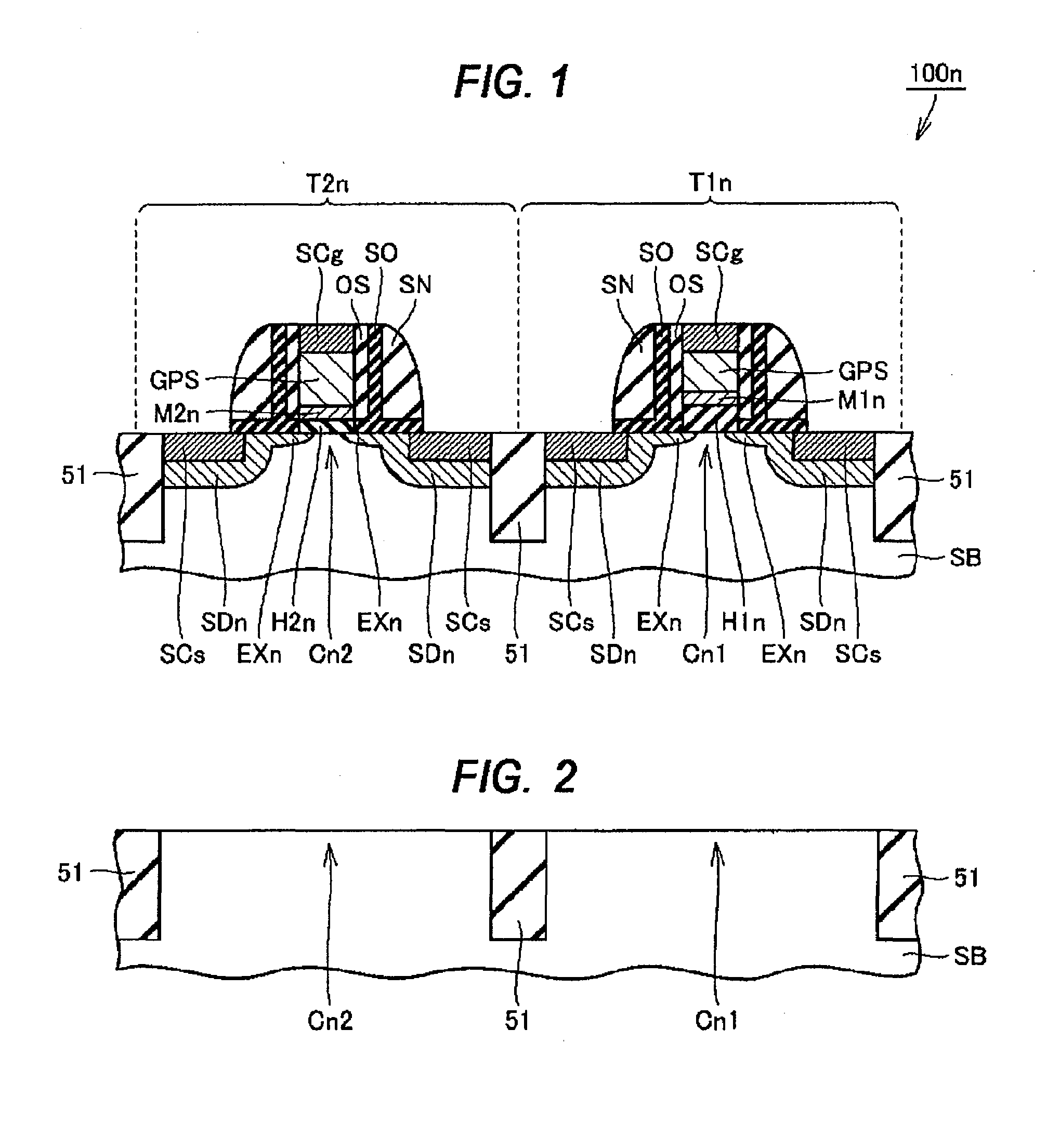
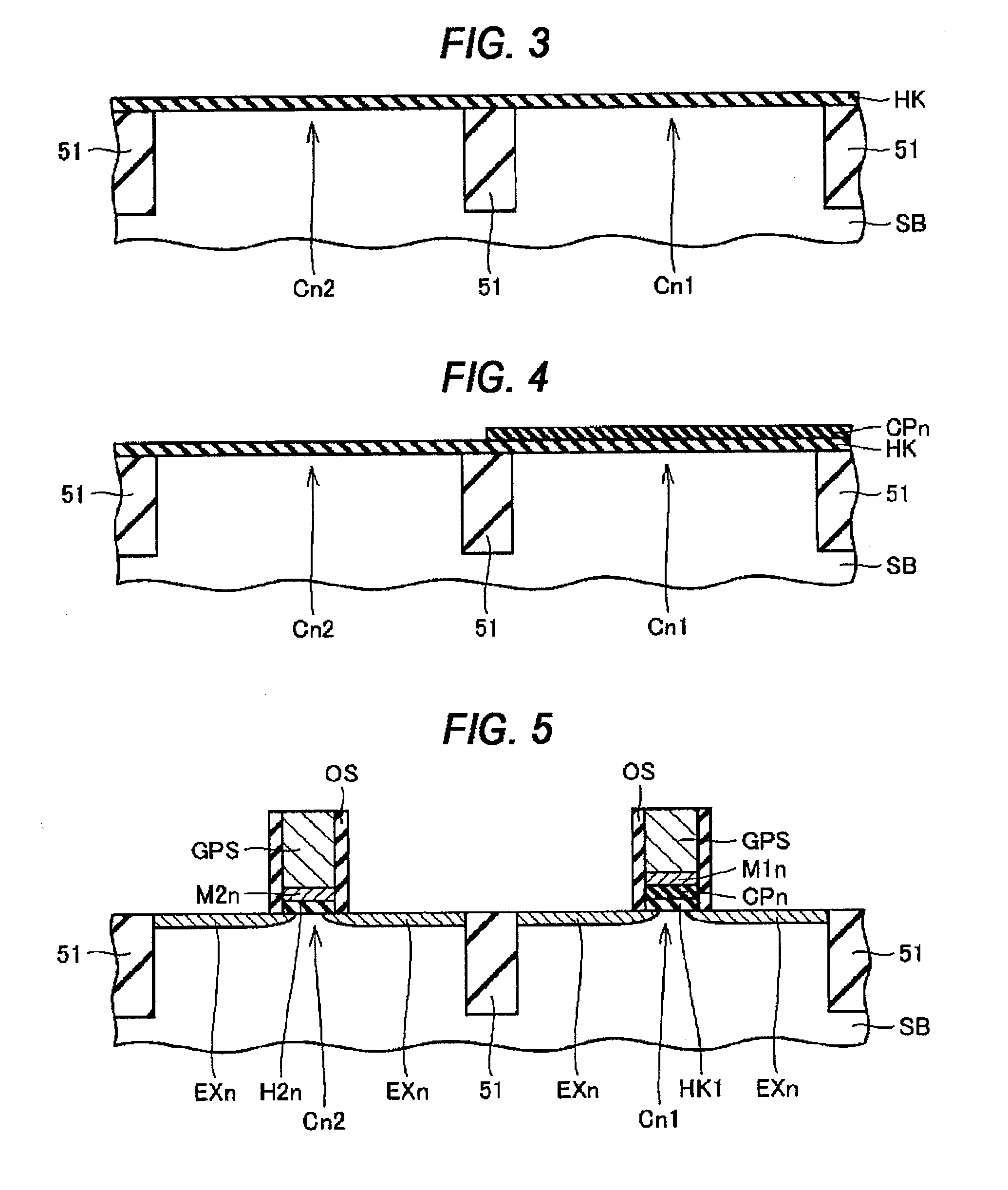
[0032]FIG. 1 is a partial section view schematically showing a configuration of a semiconductor device in a first embodiment of the present invention.

[0033]Referring to FIG. 1, a semiconductor device 100n in the present embodiment has a first nMIS transistor T1n and a second nMIS transistor T2n. The first and second nMIS transistors T1n, T2n are separated from each other by a silicon oxide film 51 configured to separate elements over a semiconductor substrate SB. The first and second nMIS transistors T1n, T2n have a first and a second nMIS threshold voltage, respectively. The absolute value of the second nMIS threshold voltage is greater than that of the first nMIS threshold voltage.

[0034]The first nMIS transistor T1n has a first nMIS channel region Cn1, a first nMIS high-k film H1n, a first nMIS metal electrode M1n, a gate polysilicon layer GPS, a pair of n-type source / drain regions SDn, an n-type source / drain extension EXn, nickel silicide layers SCg, SCs, an offset spacer OS, a s...

second embodiment

[0052]FIG. 7 is a partial section view schematically showing a configuration of a semiconductor device in a second embodiment of the present invention.

[0053]Referring to FIG. 7, a semiconductor device 100p in the present embodiment has a first pMIS transistor T1p and a second pMIS transistor T2p. The first and second pMIS transistors T1p, T2p are separated from each other by the silicon oxide film 51 configured to separate elements over the semiconductor substrate SB. The first and second pMIS transistors T1p, T2p have a first and a second pMIS threshold voltage, respectively. The absolute value of the second pMIS threshold voltage is greater than that of the first pMIS threshold voltage.

[0054]The first pMIS transistor T1p has a first pMIS channel region Cp1, a first pMIS high-k film H1p, a first pMIS metal electrode M1p, the gate polysilicon layer GPS, a pair of p-type source / drain regions SDp, a p-type source / drain extension EXp, the nickel silicide layers SCg, SCs, the offset spa...

third embodiment

[0072]FIG. 12 is a partial section view schematically showing a configuration of a semiconductor device in a third embodiment of the present invention. Referring to FIG. 12, a semiconductor device 100c in the present embodiment further has the first and second nMIS transistors T1n, T2n in addition to the configuration of the semiconductor device 100p in the second embodiment.

[0073]Configurations other than those described above are substantially the same as those in the above-described first or second embodiment, and therefore, the same symbols are assigned to the same or corresponding elements and their description is not repeated.

[0074]According to the present embodiment, the same effects as those in the first and second embodiments, respectively, can be obtained. Further, it is possible to form a CMIS structure having both the nMIS structure and the pMIS structure.


PUM


Abstract

To provide a semiconductor device and a method of manufacturing the same capable of suppressing, when a plurality of MIS transistors having different absolute values of threshold voltage is used, the reduction of the drive current of a MIS transistor having a greater absolute value of threshold voltage.
The threshold voltage of a second nMIS transistor is greater than the threshold voltage of a first nMIS transistor and the sum of the concentration of lanthanum atom and the concentration of magnesium atom in a second nMIS high-k film included in the second nMIS transistor is lower than the sum of the concentration of lanthanum atom and the concentration of magnesium atom in a first nMIS high-k film included in the first nMIS transistor.

Description

CROSS-REFERENCE TO RELATED APPLICATION[0001]The disclosure of Japanese Patent Application No. 2008-335656 filed on Dec. 29, 2008 including the specification, drawings and abstract is incorporated herein by reference in its entirety.BACKGROUND OF THE INVENTION[0002]The present invention relates to a semiconductor device and a method of manufacturing the same, in particular, relates to a semiconductor device having a plurality of MIS (Metal Insulator Semiconductor) transistors with the threshold voltages different from one another, and a method of manufacturing the same.[0003]As the film thickness of a gate insulating film is reduced in order to cope with the miniaturization of a semiconductor device, the leak current of the gate insulating film becomes a problem. In order to cope with this problem, the introduction of a high-k film as a gate insulating film material is discussed. As to the introduction, a pinning phenomenon of a threshold voltage of a MIS transistor can be a problem....

Claims


Application Information

Patent Timeline
Patent Type & Authority Applications(United States)
IPC IPC(8): H01L27/088H01L27/11H01L21/8234
CPCG11C11/412H01L21/82345H01L21/823462H01L27/11H01L27/1104H01L29/517H01L29/665H01L29/6659H01L29/7833H10B10/00H10B10/12H01L21/18H01L29/768
Inventor ONISHI, KAZUHIROTSUKAMOTO, KAZUHIRO
Owner RENESAS ELECTRONICS CORP
Why Eureka
Try Eureka