Method for manufacturing rectangular plate type chip resistor and rectangular plate type chip resistor
a technology of chip resistor and rectangular plate, which is applied in the manufacture of resistors, resistor details, resistor chips, etc., can solve the problems of insufficient reliability of electrode structure, complex production process, and insufficient adhesion of electrodes, etc., to achieve high-reliable electrode structure, low cost, and efficient manufacture of reliable chip resistors
- Summary
- Abstract
- Description
- Claims
- Application Information
AI Technical Summary
Benefits of technology
Problems solved by technology
Method used
Image
Examples
example 1
Manufacture of Resistor of Desired Resistance 1 mΩ
[0052]Resistive copper-manganese-tin (Cu—Mn—Sn) alloy plate strips (volume resistivity 0.30 μΩ·m), which had been adjusted to the length of about 30 cm, the width of 6.3 mm±0.25 mm, and the thickness of 0.23±0.07 mm, were provided. The alloy plate strips were subjected in advance to degreasing with a persulfate type liquid and roughening for improving adhesion of the protective film to be discussed later.
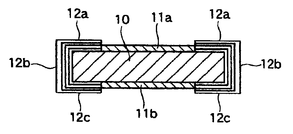
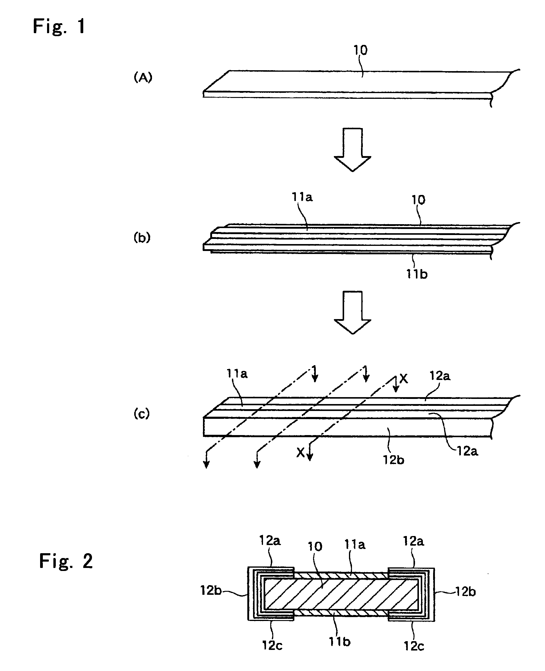
[0053]Next, an insulating protective film was screen printed along the middle of the upper and lower faces of each alloy plate strip as shown in FIG. 1(B) so as to have a width of 1.9 mm±0.25 mm and a thickness of about 20 μm, baked at 200° C., and subjected to removal of an oxide film.
[0054]Each of the resulting alloy plate strip was subjected to nickel strike plating at a current density of 6 A / dm2 in a Wood's bath at 20° C. containing 240 g / L of nickel chloride and 100 ml / L of concentrated hydrochloric acid for 5 minutes. As a res...
example 2
Manufacture of Resistor of Desired Resistance 10 mΩ
[0060]Resistive iron-chromium-aluminum (Fe—Cr—Al) alloy plate strips (volume resistivity 1.30 μΩ·m), which had been adjusted to the length of about 30 cm, the width of 6.3 mm±0.25 mm, and the thickness of 0.20 mm±0.07 mm, were provided. The alloy plate strips were subjected in advance to degreasing with a ferric chloride type liquid and roughening for improving adhesion of the protective film to be discussed later.
[0061]Next, an insulating protective film was screen printed along the middle of the upper and lower faces of each alloy plate strip as shown in FIG. 1(B) so as to have a width of 4.3 mm±0.25 mm and a thickness of about 20 μm, baked at 200° C., and subjected to removal of an oxide film.
[0062]Each of the resulting alloy plate strip was subjected to nickel strike plating at a current density of 6 A / dm2 in a Wood's bath at 20° C. containing 240 g / L of nickel chloride and 100 ml / L of concentrated hydrochloric acid for 5 minute...
PUM
 Abstract
Description
Claims
Application Information

