

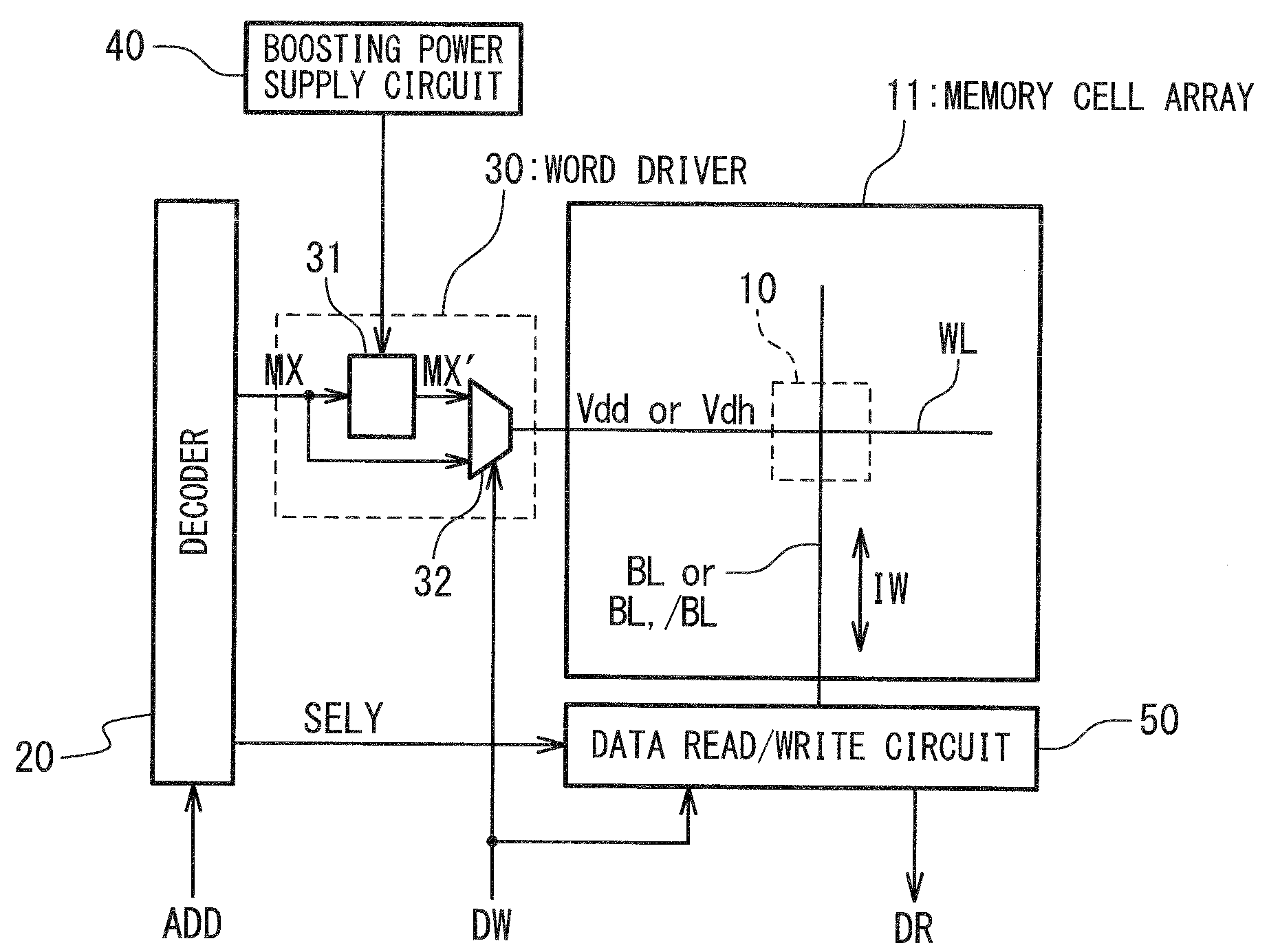
MRAM having variable word line drive potential
a variable word line drive and variable word technology, applied in the field of magnetic random access memory (mram), can solve the problems of deteriorating quality of read signal, difficult to accurately read data, and difficulty in supplying sufficient write current iw over the threshold, so as to reduce the resistance of selection transistor, increase the supply of write current, and increase the capacity of mram
- Summary
- Abstract
- Description
- Claims
- Application Information
AI Technical Summary
Benefits of technology
Problems solved by technology
Method used
Image

Examples
first exemplary embodiment
1. First Exemplary Embodiment
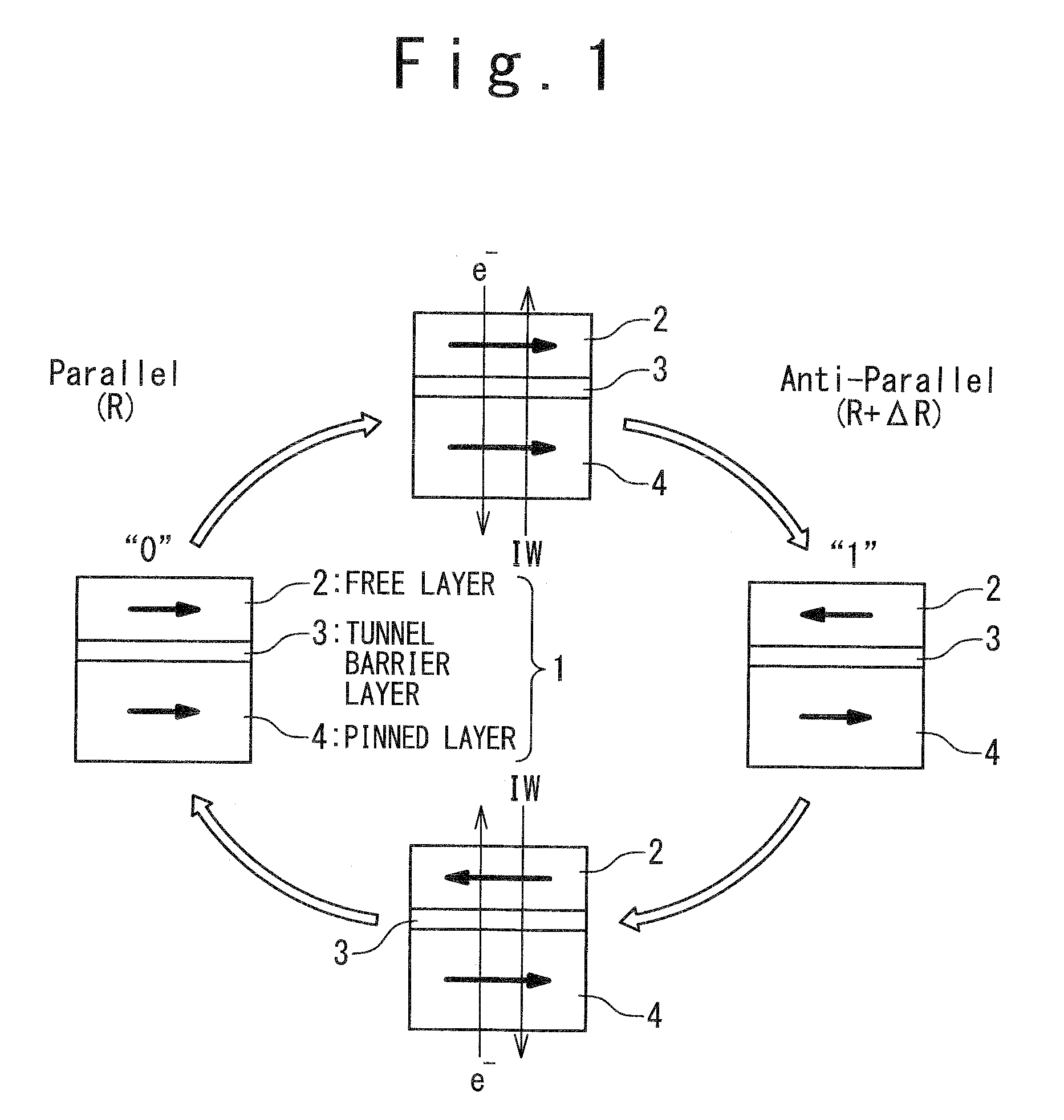
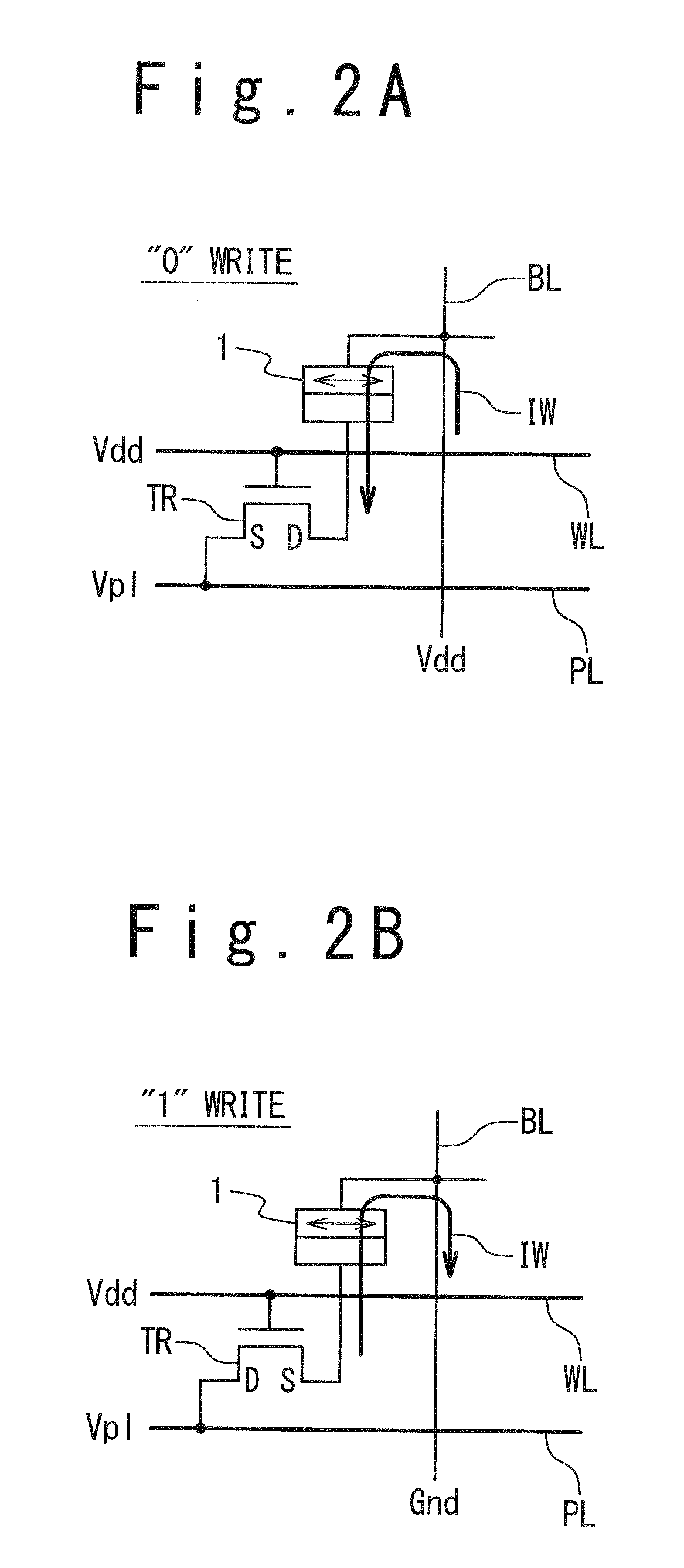
[0033]FIG. 3A and FIG. 3B are schematic diagrams showing the configuration and data write of a memory cell 10a according to a first exemplary embodiment. The memory cell 10a contains an MTJ element 1 and a selection transistor (cell transistor) TR. The selection transistor TR is a MOS transistor.
[0034]The MTJ element 1 has a structure similar to the structure shown in FIG. 1. That is, the MTJ element 1 has a bottom pin structure in which a free layer 2 is formed through a tunnel barrier layer 3 on a pinned layer 4. In FIG. 3A and FIG. 3B, the magnetization of the free layer 2 is indicated by an arrow mark. One end of the MTJ element 1 is connect a bit line BL, and the other end thereof is connected to the selection transistor TR. In detail, the free layer 2 of the MTJ element 1 is connected to the bit line BL, and the pinned layer 4 is connected to one of source / drain electrodes of the selection transistor TR.
[0035]A gate electrode of the selection trans...
second exemplary embodiment
2. Second Exemplary Embodiment
[0043]FIG. 4A and FIG. 4B are schematic diagrams showing the configuration of a memory cell 10b and data write, according to the second exemplary embodiment. Hereinafter, the same description as that in the first exemplary embodiment is properly omitted.
[0044]One end of the MTJ element is connected to the plate line PL, and the other end thereof is connected to the selection transistor TR. In detail, the free layer 2 of the MTJ element 1 is connected to the plate line PL, and the pinned layer 4 is connected to one of the source / drain electrodes of the selection transistor TR. The other of the source / drain electrodes of the selection transistor TR is connected to the word line WL.
[0045]FIG. 4A shows the “0” write into the memory cell 10b. When “0” is written, the word line WL is driven with the power supply voltage Vdd, and the power supply voltage Vdd is applied to the gate electrode of the selection transistor TR. The ground voltage Gnd lower than the ...
third exemplary embodiment
3. Third Exemplary Embodiment
[0050]FIG. 5A and FIG. 5B are schematic diagrams showing the configuration of a memory cell 10c and data write, according to the third exemplary embodiment. Hereinafter, the same description as that in the first exemplary embodiment is properly omitted.
[0051]The gate electrode of the selection transistor TR is connected to the word line WL. One of the source / drain electrodes of the selection transistor TR is connected to a first bit line BL, and the other thereof is connected to one end (pinned layer 4) of the MTJ element 1. The other end (free layer 2) of the MTJ element 1 is connected to a second bit line / BL. The first bit line BL and the second bit line / BL configure a complementary bit line pair. In short, when the power supply voltage Vdd is applied to the first bit line BL, the ground voltage Gnd is applied to the second bit line / BL. When the ground voltage Gnd is applied to the first bit line BL, the power supply voltage Vdd is applied to the se...
PUM
 Abstract
Description
Claims
Application Information