

Plasma atomic layer deposition system and method
a technology of atomic layer and plasma, which is applied in the direction of plasma technique, metal material coating process, coating, etc., can solve the problems of preventing rapid deployment and advancement of ald and pald coating systems, reducing coating throughput, and self-limiting of ald coating processes.
- Summary
- Abstract
- Description
- Claims
- Application Information
AI Technical Summary
Benefits of technology
Problems solved by technology
Method used
Image

Examples
Embodiment Construction
7.1 Overview
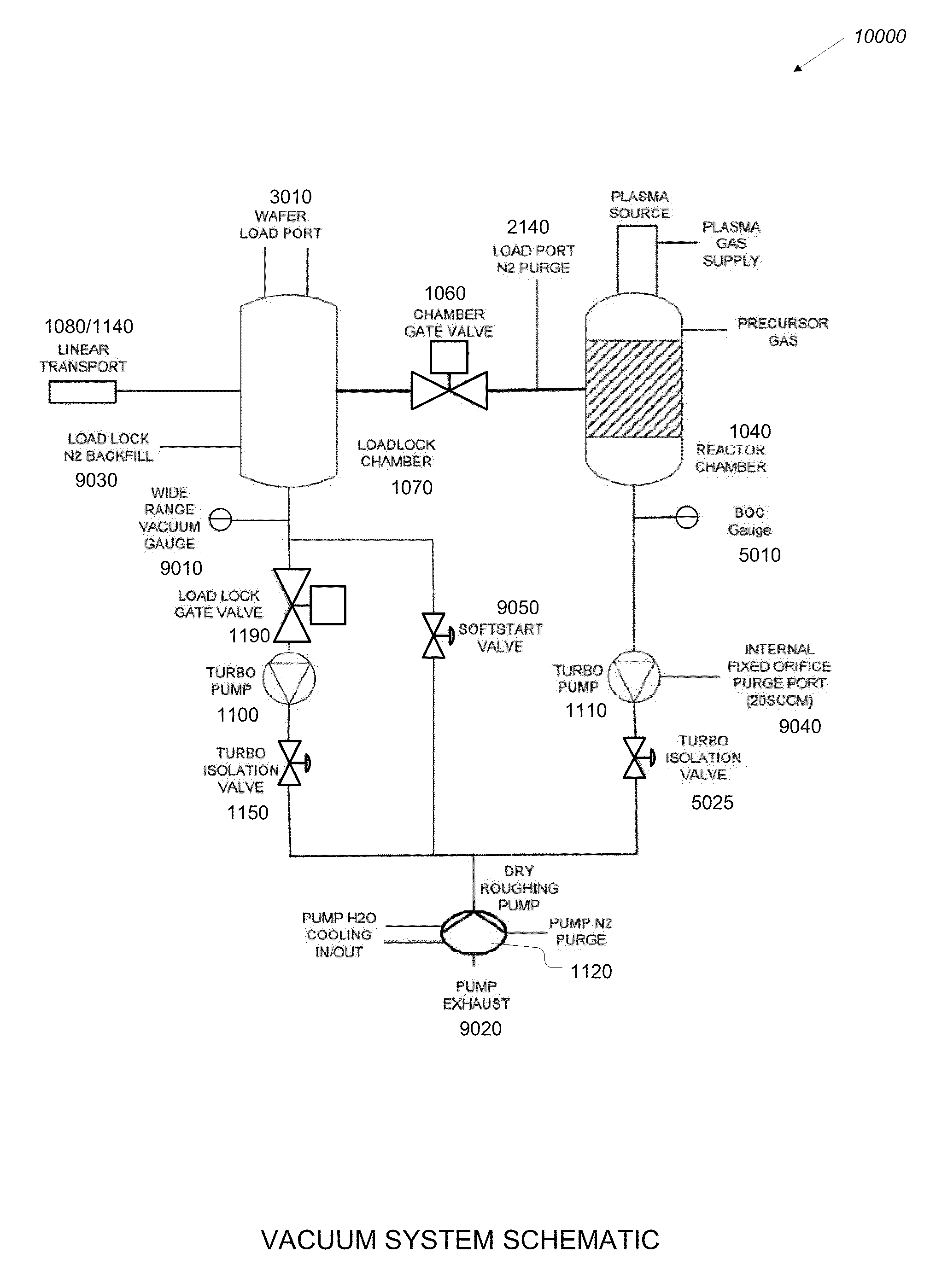
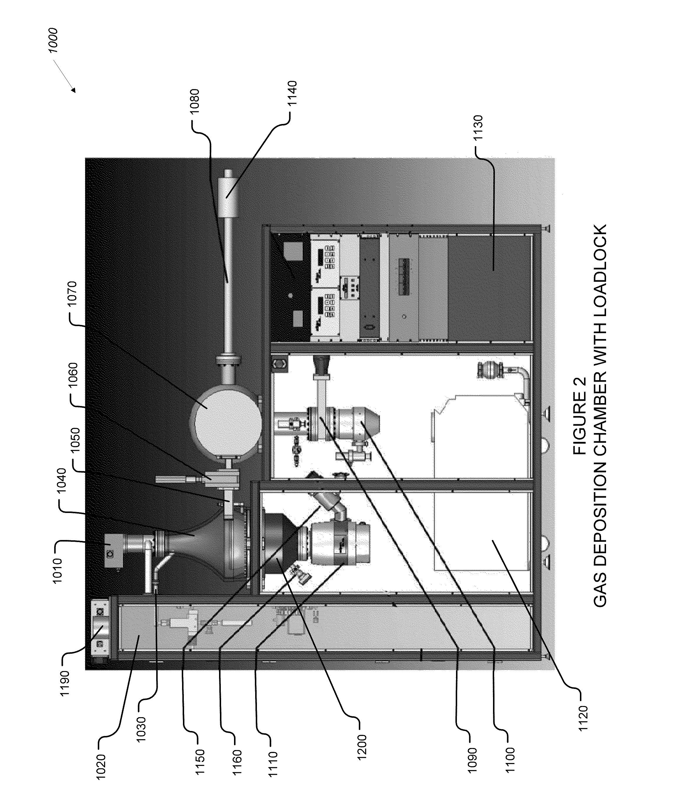
[0050]The present invention is a gas deposition system configured to deposit thin films onto substrate surfaces by several gas deposition processes. In particular, the gas deposition system of the present invention is configured as a plasma assisted or plasma enhanced atomic layer deposition (PALD) system, which includes a plasma source. The plasma source is suitable for delivering a plurality of different plasma excited gases into a gas deposition or reaction chamber. In addition, the gas deposition system of the present invention is configured as a conventional atomic layer deposition (ALD) system suitable for delivering a plurality of different ALD precursors or reactants into the gas deposition or reaction chamber. One advantage of the PALD aspect of the present invention is that a PALD gas deposition system can be used to deposit thin film material types that are not able to be deposited by the conventional or thermal ALD process and therefore not able to be deposit...
PUM
| Property | Measurement | Unit |
|---|---|---|
| diameter | aaaaa | aaaaa |
| operating pressure | aaaaa | aaaaa |
| vacuum pressure | aaaaa | aaaaa |
Abstract
Description
Claims
Application Information