Semiconductor device, method of manufacturing the same, and electronic apparatus

Active Publication Date: 2010-08-05
SONY SEMICON SOLUTIONS CORP
View PDF15 Cites 14 Cited by
  • Summary
  • Abstract
  • Description
  • Claims
  • Application Information

AI Technical Summary

Benefits of technology

[0019]In the semiconductor device according to the embodiment of the present invention, in the structure of the device substrate, the hole is formed in the second surface opposite to the first surface on which the transistor is formed. With this structure, in a case where the semiconductor device is manufactured, hydrogen is supplied from the second surface of the device substrate through the hole. As a result, hydrogen more easily reaches the gate insulating film of the transistor as compared to the case where the hole is not formed.
[0020]According to the embodiment of the present invention, it is possible to supply

Problems solved by technology

As a result, it becomes difficult to handle the semiconductor substrate in subsequent processes.
Further, if the semiconductor substrate is ground or

Method used


Image

  • Semiconductor device, method of manufacturing the same, and electronic apparatus
  • Semiconductor device, method of manufacturing the same, and electronic apparatus
  • Semiconductor device, method of manufacturing the same, and electronic apparatus

Examples


Example

1. First Embodiment

(Structure of Semiconductor Device)

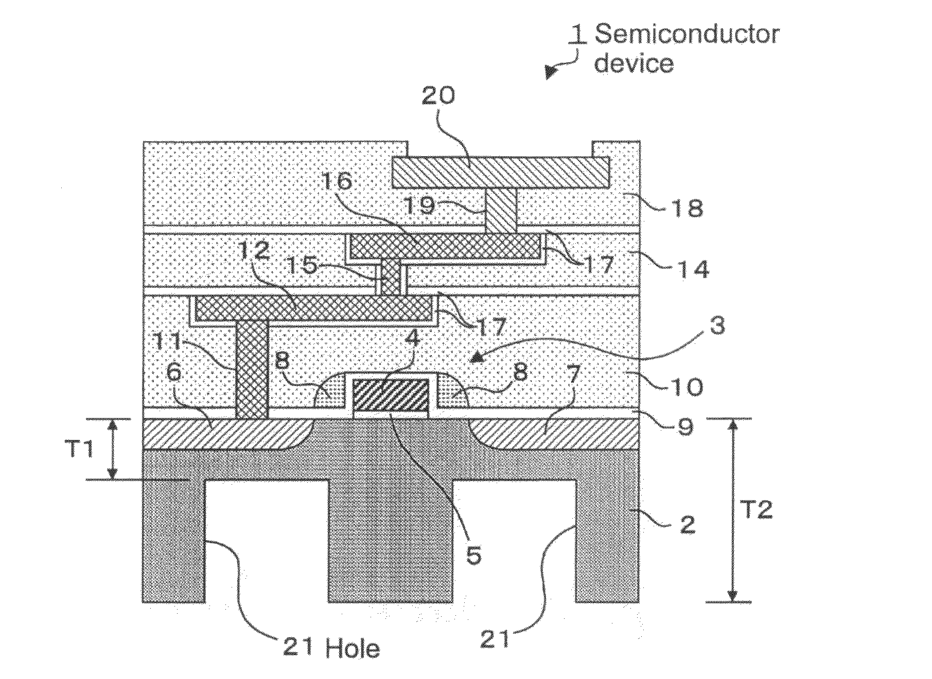
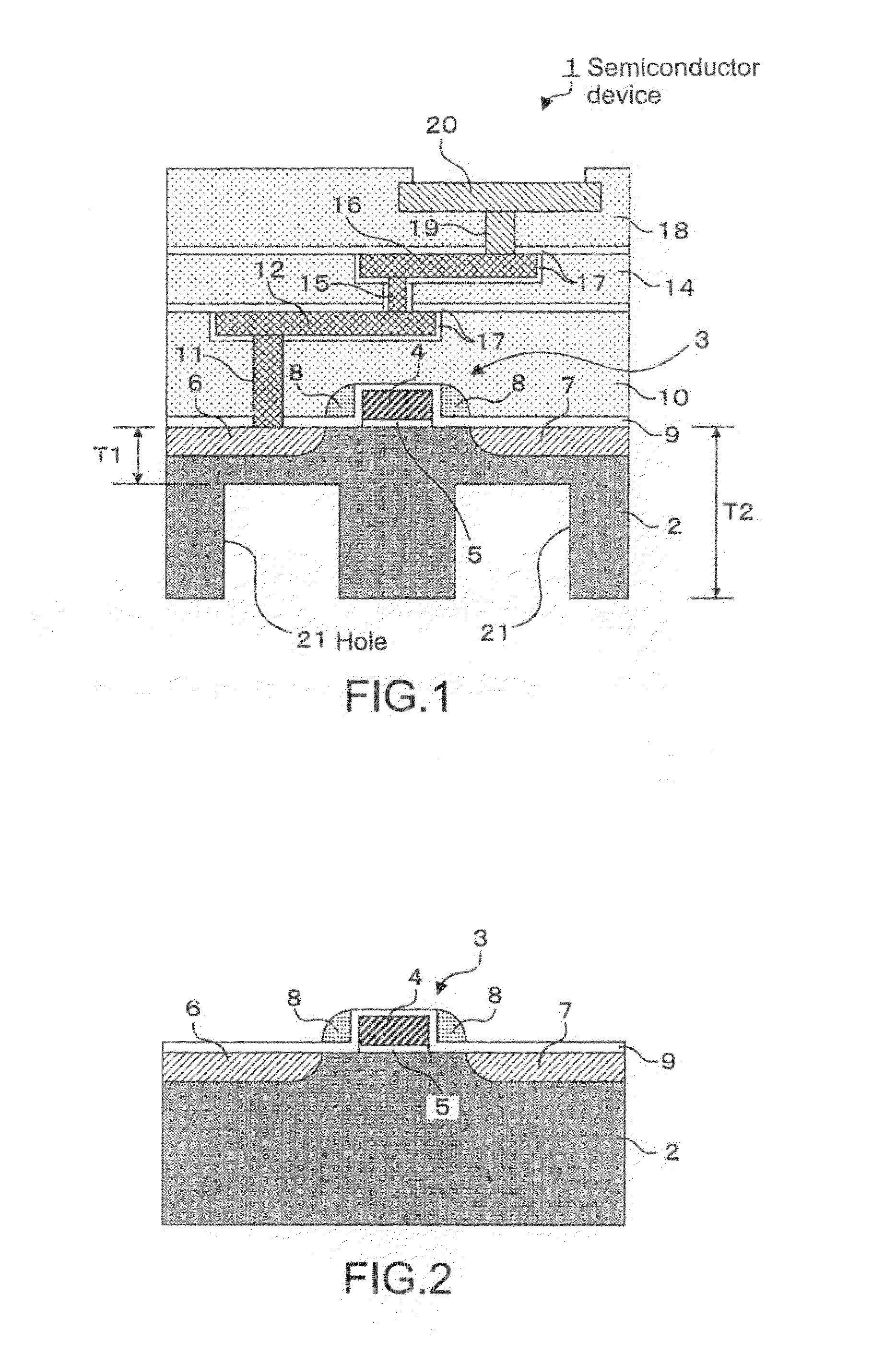
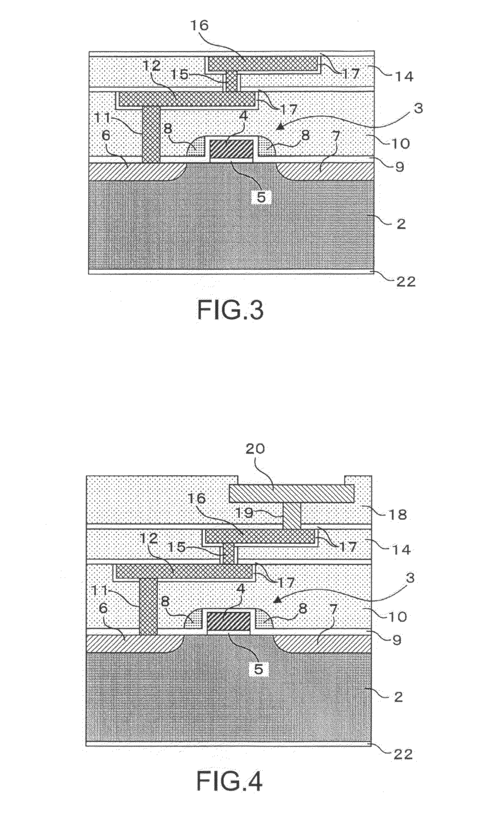
[0043]FIG. 1 is a cross-sectional view showing a structure of a semiconductor device according to a first embodiment of the present invention. A semiconductor device 1 shown in FIG. 1 includes a semiconductor substrate 2 as a device substrate. The semiconductor substrate 2 is formed of a silicon substrate that is a P-type semiconductor substrate. On a first surface (upper surface) of the semiconductor substrate 2, a transistor is formed. The transistor 3 is constituted of a gate electrode 4, a gate insulating film 5, a source region 6, and a drain region 7. The gate electrode 4 is formed on the gate insulating film 5. The gate electrode 4 is made of polysilicon, for example. The gate insulating film 5 is intervened between the gate electrode 4 and the semiconductor substrate 2. The gate insulating film 5 is made of a silicon oxide film, for example. On both side surfaces of the gate electrode 4, sidewalls 8 are formed. The source...

Example

2. Second Embodiment

[0058]FIG. 10 is a cross-sectional view showing a structure of a semiconductor device according to a second embodiment of the present invention. The semiconductor device 1 shown in FIG. 10 includes a glass substrate 25 as a device substrate. On a first surface (upper surface) of the glass substrate 25, a polysilicon thin film 26 is formed. On the polysilicon thin film 26, the source region 6 and the drain region 7 of the transistor 3 are formed. In a second surface (lower surface) of the glass substrate 25, a plurality of holes 27 are formed under the same condition as in the case of the semiconductor substrate 2 described above. The plurality of holes 27 are formed for the same purpose as the holes 21. The other structure, basic manufacturing processes (manufacturing method), and operations and effects are the same as in the first embodiment, and therefore their descriptions will be omitted. It should be noted that the glass substrate is used as the device subst...

Example

3. Third Embodiment

[0059]FIG. 11 is a cross-sectional view showing a structure of a semiconductor device according to a third embodiment of the present invention. The semiconductor device 1 shown in FIG. 11 includes an SOI substrate 28 as a device substrate. The SOI substrate 28 is constituted of a silicon substrate 29 as a base, a BOX oxide film 30, and a crystalline silicon thin film 31. The BOX oxide film 30 is formed of a silicon oxide film. The BOX oxide film 30 and the crystalline silicon thin film 31 are formed on a surface (upper surface) of the silicon substrate 29 in a laminated manner in the stated order. Of those, in the crystalline silicon thin film 31, the source and drain regions 6 and 7 of the transistor 3 are formed. Further, on the other surface (lower surface) of the silicon substrate 29 corresponding to the second surface of the SOI substrate 28, a plurality of holes 32 are formed under the same condition as in the case of the semiconductor substrate 2 described ...


PUM


Abstract

Disclosed is a method of manufacturing a semiconductor device including forming a transistor on a first surface of a device substrate, forming a hole in a second surface opposite to the first surface of the device substrate, and supplying hydrogen to a gate insulating film of the transistor from the second surface of the device substrate through the hole.

Description

BACKGROUND OF THE INVENTION[0001]1. Field of the Invention[0002]The present invention relates to a semiconductor device including a transistor, a method of manufacturing a semiconductor device, and an electronic apparatus.[0003]2. Description of the Related Art[0004]As a form of a semiconductor device, a solid-state image sensor is known. Examples of a typical solid-state image sensor include a CCD image sensor and a CMOS image sensor. The solid-state image sensor of this type has a noise characteristic as a pixel characteristic. Noises of a solid-state image sensor are roughly classified into a random noise and a fixed pattern noise. Further, examples of a typical random noise include a dark current shot noise, an FD (floating diffusion) reset noise, an FD amplifier noise, and a light shot noise.[0005]Further, causes of the noise arise from the following items (1) to (4):[0006](1) a deep level of a forbidden band of silicon,[0007](2) a thermal noise in a case where a capacitance C ...

Claims


Application Information

Patent Timeline
IPC IPC(8): H01L23/00H01L21/50
CPCH01L27/14609H01L27/14612H01L29/78H01L27/14689
Inventor NAKAMURA, AKIHIRO
Owner SONY SEMICON SOLUTIONS CORP
Why Eureka
Try Eureka