Semiconductor device and method for manufacturing same

a semiconductor and wire technology, applied in the direction of semiconductor devices, semiconductor/solid-state device details, electrical apparatus, etc., can solve the problems of serious disconnection defects in copper wiring, difficulty in dry etching processing, and reduced processing efficiency, so as to improve the adhesion of copper wires and barrier metal films, the effect of enhancing the resistance to stress migration and enhancing the electromigration resistan

Active Publication Date: 2010-08-05
GK BRIDGE 1
View PDF6 Cites 16 Cited by
  • Summary
  • Abstract
  • Description
  • Claims
  • Application Information

AI Technical Summary

Benefits of technology

[0026]Adhesion of the copper wiring and the barrier metal film can be enhanced, and electromigration resistance and stress migration resistance can be enhanced through the use of the semiconductor device and the method for manufacturing the semiconductor device according to the present invention.

Problems solved by technology

Since processing by dry etching is difficult, a damascene method is generally used when the copper wiring is formed.
The dimensions of wiring have become smaller in recent years in conjunction with LSI miniaturization, and disconnection defects in copper wiring are a serious problem.
Copper migration is a contributing factor to wiring disconnection defects.

Method used


Image

  • Semiconductor device and method for manufacturing same
  • Semiconductor device and method for manufacturing same
  • Semiconductor device and method for manufacturing same

Examples


embodiment 1

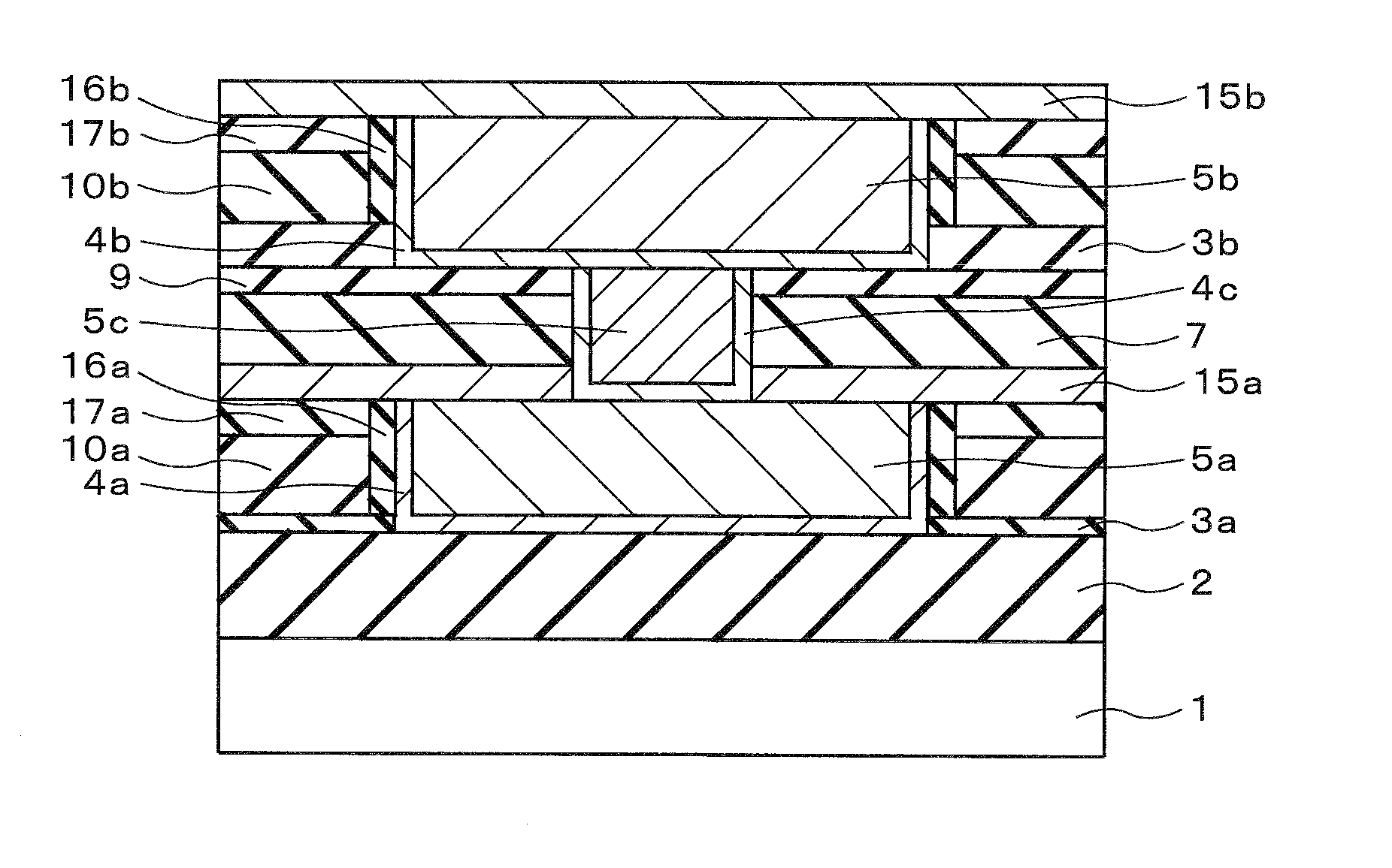
[0072]The wiring structure according to Embodiment 1 of the present invention will be described using FIG. 3. Embodiment 1 of the present invention is an embodiment in which the present invention is applied to dual damascene wiring.

[0073]As shown in FIG. 3, in the wiring structure according to Embodiment 1 of the present invention, a wiring structure is formed in which an interlayer insulation film 2 and an etch-stop film 3a are layered on a semiconductor substrate 1 on which a semiconductor element (not shown) is formed, copper or copper alloy wiring 5a surrounded by a barrier metal film 4a is formed by a damascene method on the upper part of the etch-stop film 3a, and the upper surface of the wiring is covered by a wiring protective film 6a. A via interlayer insulation film 7 and an etch-stop film 3b are layered on the upper layer, and a via and wiring are formed by a dual damascene method. A wiring structure is formed in which the via and wiring are composed of copper or copper a...

embodiment 2

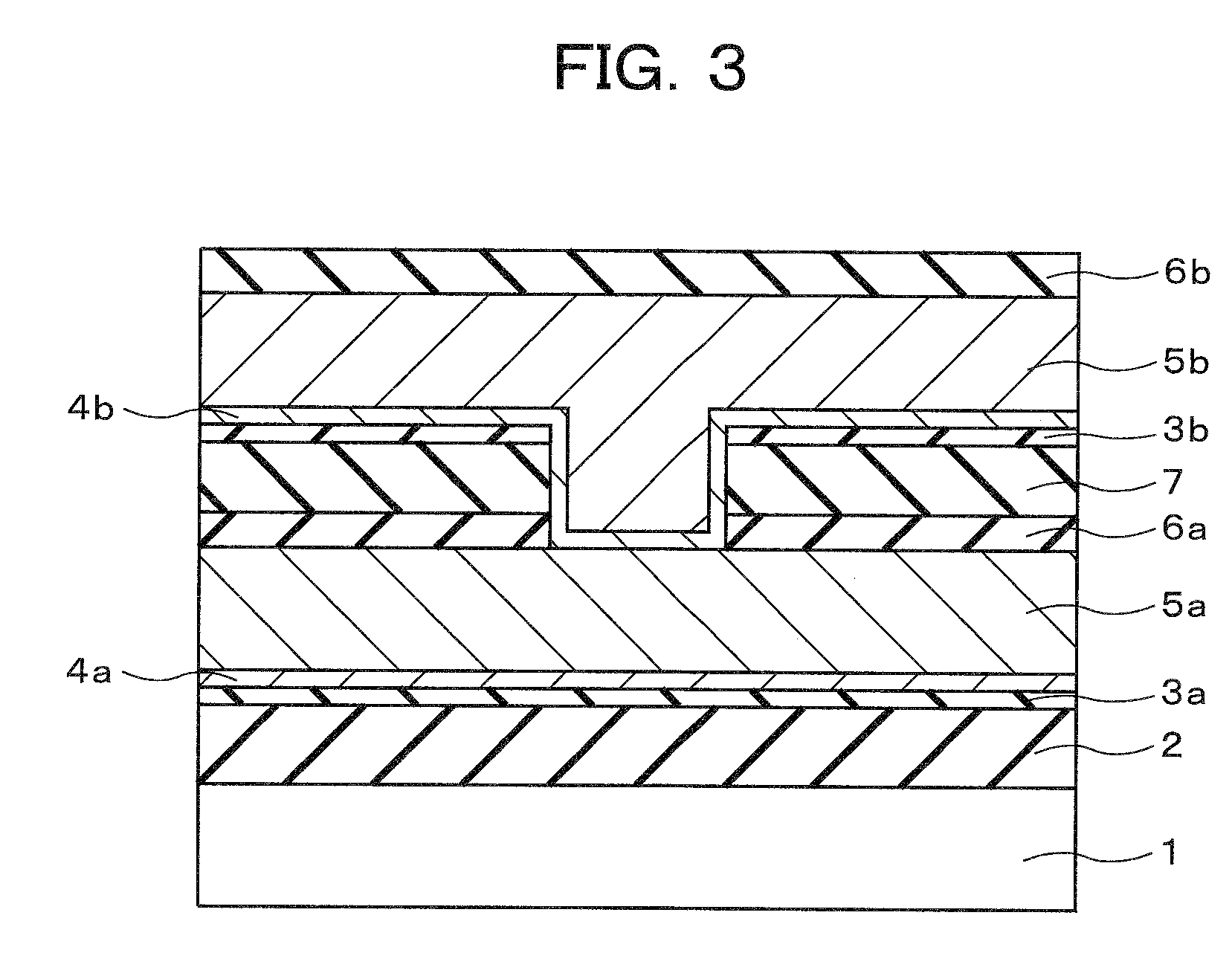
[0102]The wiring structure according to Embodiment 2 of the present invention will be described with reference to FIG. 5. Embodiment 2 of the present invention is an embodiment in which the present invention is applied to single damascene wiring.

[0103]As shown in FIG. 5, in the wiring structure according to Embodiment 2 of the present invention, a wiring structure is formed in which the interlayer insulation film 2 and the etch-stop film 3a are layered on the semiconductor substrate 1 in which a semiconductor element (not shown) is formed, copper or copper alloy wiring 5a surrounded by the barrier metal film 4a is formed by a single damascene method in the upper part, and the upper surface of the wiring is covered by the wiring protective film 6a. On the upper layer thereof, the via interlayer insulation film 7 and a via-layer hard mask 9 are layered, and a via is formed in the inside by the single damascene method. The via is formed by a copper or copper alloy via 5c that is surrou...

example 1

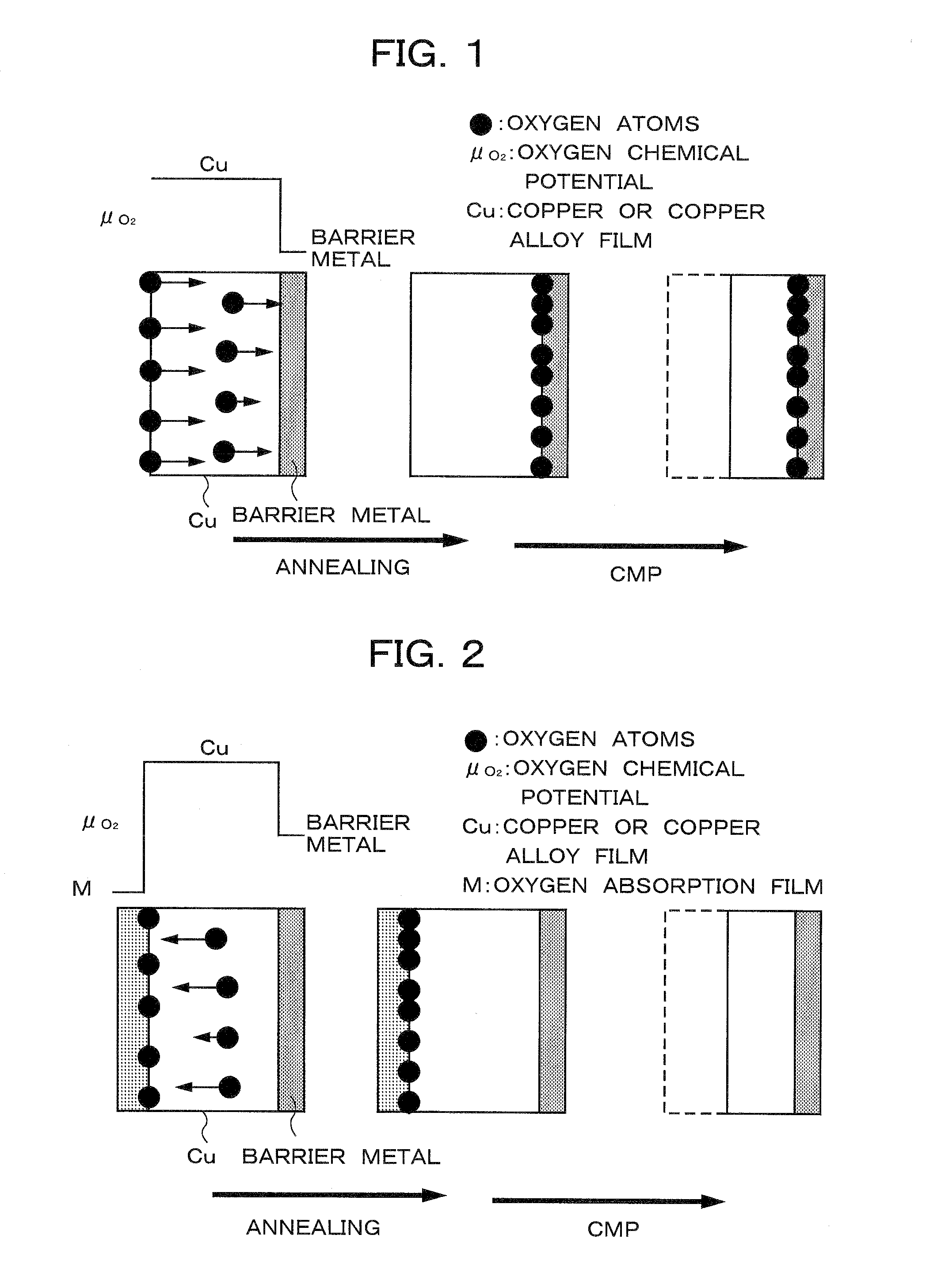
[0130]An example of the present invention will be described using FIG. 7. FIG. 7 shows the oxygen concentration profile in the films when the Ta / TaN layered film is formed as the barrier metal film, and the copper seed film, the copper plating film, and the oxygen absorption film composed of an Al thin film having a thickness of 3 nm are formed in sequence on the upper surface, and the assembly is heated at 350° C. in the manufacturing steps shown in FIGS. 4E and 6E. The oxygen concentration profile in the conventional structure in which heat is applied without forming the oxygen absorption film is also shown simultaneously as a comparative example. The lesser depth is towards the Cu plating film. A case is shown in which the barrier metal film is formed on the silicon oxide film formed on the silicon substrate, and the oxygen concentration profile is calculated by SIMS analysis from the side of the back surface of the substrate. Therefore, oxygen is detected inside the barrier meta...


PUM

PropertyMeasurementUnit
temperatureaaaaaaaaaa

Abstract

A trench is formed in an insulation film formed on top of a semiconductor substrate, and a barrier metal film is formed on the surface of the trench. After a copper or copper alloy film is formed on the barrier metal film, an oxygen absorption film in which a standard energy of formation of an oxidation reaction in a range from room temperature to 400° C. is negative, and in which an absolute value of the standard energy of formation is larger than that of the barrier metal film is formed, and the assembly is heated in a temperature range of 200 to 400° C. A semiconductor device can thereby be provided that has highly reliable wiring, in which the adhesion to the barrier metal film in the copper interface is enhanced, copper diffusion in the interface is suppressed, and electromigration and stress migration are prevented.

Description

TECHNICAL FIELD[0001]The present invention relates to a semiconductor device having wiring, and particularly relates to a semiconductor device composed of a trench wiring (damascene wiring) structure having copper as the primary component, and to a method for manufacturing the semiconductor device.BACKGROUND ART[0002]Aluminum (Al) or Al alloy has been widely used in the past as the conductive material in silicon semiconductor integrated circuits (LSI). Copper (Cu) has come to be used as the conductive material in order to increase reliability and reduce wiring resistance in the wiring in conjunction with advances in LSI miniaturization.[0003]Since processing by dry etching is difficult, a damascene method is generally used when the copper wiring is formed. The damascene method is a method whereby copper is filled into a wiring trench and / or a via formed in an insulation film on the semiconductor substrate, and wiring is formed by polishing off and removing the excess copper.[0004]Th...

Claims


Application Information

Patent Timeline
Patent Type & Authority Applications(United States)
IPC IPC(8): H01L23/532H01L21/768
CPCH01L21/76807H01L21/76831H01L21/76835H01L21/76841H01L21/76873H01L21/76877H01L21/76883H01L2924/0002H01L23/53233H01L23/53238H01L2221/1036H01L2924/00
Inventor AMANO, MARITADA, MUNEHIROFURUTAKE, NAOYAHAYASHI, YOSHIHIRO
Owner GK BRIDGE 1
Why Eureka
Try Eureka