Method of forming metal wiring and metal wiring formed using the same

a technology of metal wiring and metal wiring, which is applied in the direction of resistive material coating, metallic pattern materials, metallic material coating processes, etc., can solve the problems of difficult to quickly apply a new design to a production line, difficult to achieve the same design quickly, and difficult to achieve the same design. , to achieve the effect of improving the electrical and mechanical characteristics and stable fine structur

Inactive Publication Date: 2010-08-05
SAMSUNG ELECTRO MECHANICS CO LTD
View PDF2 Cites 8 Cited by
  • Summary
  • Abstract
  • Description
  • Claims
  • Application Information

AI Technical Summary

Benefits of technology

[0010]An aspect of the present invention provides a method of forming metal wiring using metallic nanoparticles, which can achieve superior electrical and mechanical characteristics by forming a stable fine structure.
[0011]According to an aspect of the present invention, there is provided a method of forming metal wiring, the method including: printing wiring using an ink composition including metallic nanoparticles and dispersants maintaining dispersion of the metallic nanoparticles; performing a first firing process of firing the wiring under vacuum or in an inert atmosphere to suppress grain growth; and performing a second firing process of firing the wiring with the vacuum or inert atmosphere released, to accelerate grain growth.

Problems solved by technology

However, this optical patterning method is wasteful of materials and requires complicated multistage processes due to the use of photoresist, developer or etching solution for example, thus imparing process efficiency.
Moreover, a large mask needs to be used in the optical patterning process, and this makes it difficult to quickly apply a new design to a production line.
Thus, the selection of the wiring material is an important issue.

Method used


Image

  • Method of forming metal wiring and metal wiring formed using the same
  • Method of forming metal wiring and metal wiring formed using the same
  • Method of forming metal wiring and metal wiring formed using the same

Examples


embodiments

Embodiment 1

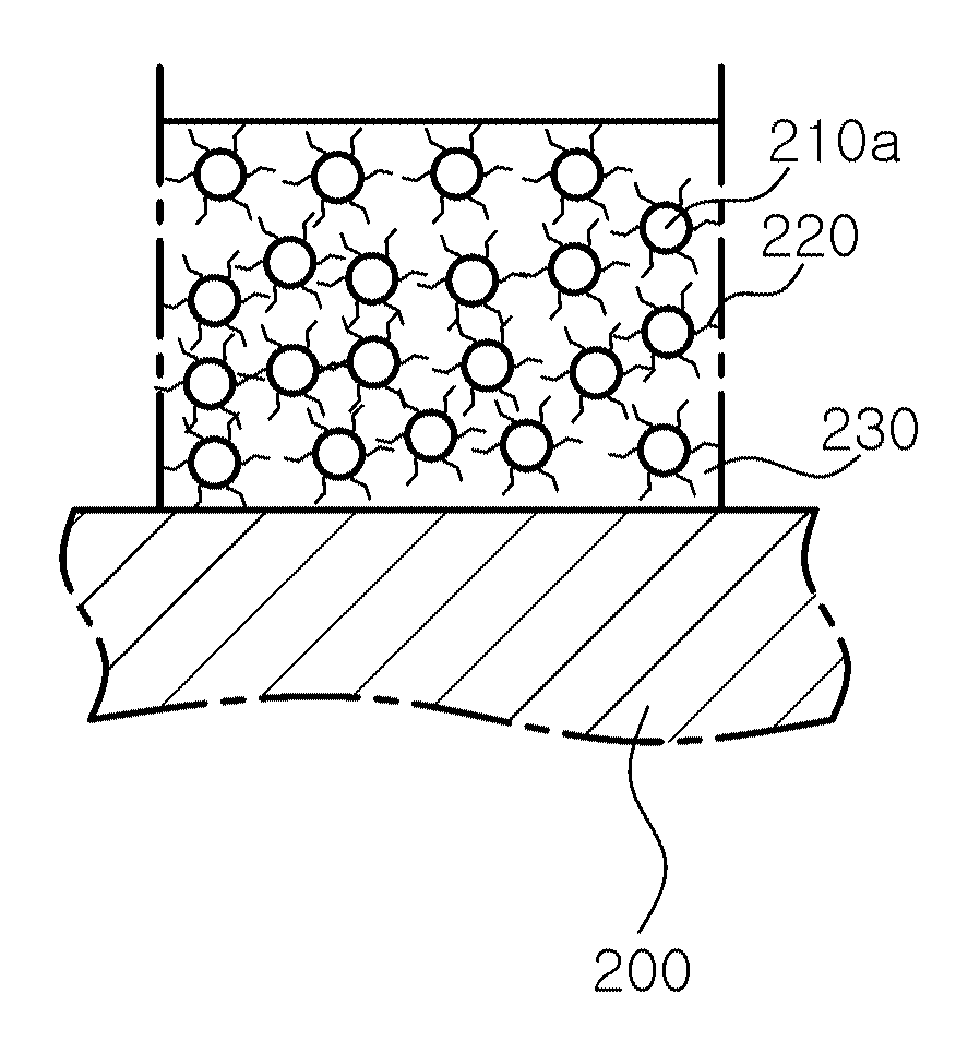
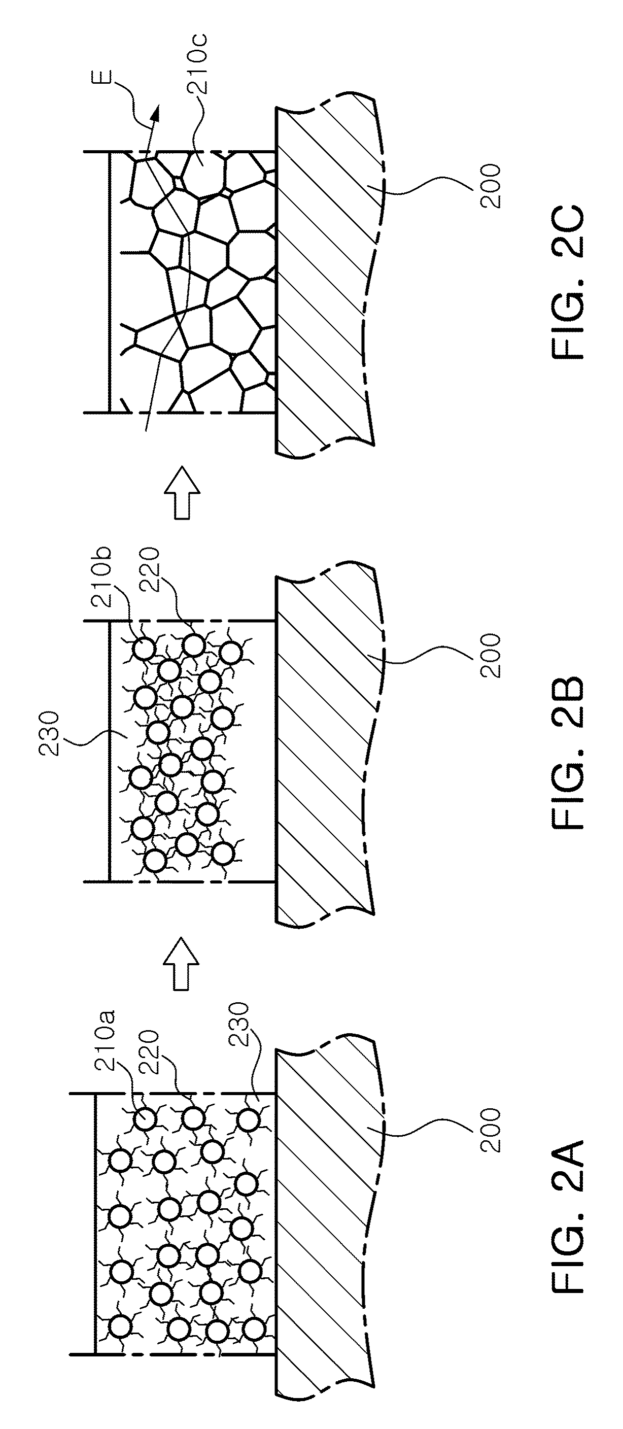
[0052]Metal wiring was printed on a substrate by an inkjet printing method, using ink containing Ag nanoparticles (40 wt %). A printing test piece was put into a vacuum oven and the temperature was increased up to 250° C. at a heating rate of 3° C. / min in the vacuum state. Thereafter, air was introduced into the vacuum oven, and firing was performed at 250° C. for about two hours. FIG. 3 is an SEM image showing a cross-section of wiring obtained by the embodiment 1. As shown in FIG. 3, the metallic nanoparticles have a coarse-grained structure. Although pores are present due to the gasification of the dispersants within a film, the pores have no significant influence on electrical and mechanical characteristics because they are unconnected to one another. Specific resistance was calculated by measuring surface resistance using a surface measuring device (4 point probe), and then measuring thickness. The specific resistance was 5.32 μΩ·cm.

embodiment 2

[0053]The printing test piece, fabricated by the above embodiment 1, was fired at 250° C. for about 30 minutes under a pressure of 5 Mpa or higher. FIGS. 4A and 4B are SEM images showing the top of wiring according to the embodiment 2. FIG. 4A is an image before firing, and FIG. 4B is an image after the firing. Referring to FIGS. 4A and 4B, the metallic nanoparticles increase in size, and bonding between the particles is enhanced. A result of measuring an elongation according to Japan industrial standard (JIS) showed that the elongation is increased from 1.4% to 2.8%.


PUM

PropertyMeasurementUnit
particle sizeaaaaaaaaaa
temperatureaaaaaaaaaa
pressureaaaaaaaaaa

Abstract

Disclosed are a method of forming metal wiring and metal wiring formed using the same. The method includes printing wiring using an ink composition including metallic nanoparticles and dispersants maintaining dispersion of the metallic nanoparticles, performing a first firing process of firing the wiring under vacuum or in an inert atmosphere to suppress grain growth, and performing a second firing process of firing the wiring with the vacuum or inert atmosphere released, to accelerate grain growth. The method of forming metal wiring induces abnormal grain growth by rapidly removing dispersants, capable of inducing the growth of metallic nanoparticles, at a temperature at which the growth force of the metallic nanoparticles is high, in the process of firing the metallic nanoparticles. Accordingly, the metal wiring has a coarse-grained structure containing metallic particles with a large average particle size, and the electrical and mechanical characteristics thereof can be enhanced.

Description

CROSS-REFERENCE TO RELATED APPLICATIONS[0001]This application claims the priority of Korean Patent Application No. 2009-0008492 filed on Feb. 3, 2009, in the Korean Intellectual Property Office, the disclosure of which is incorporated herein by reference.BACKGROUND OF THE INVENTION[0002]1. Field of the Invention[0003]The present invention relates to a method of forming metal wiring and metal wiring formed using the same, and more particularly, to a method of forming metal wiring and metal wiring formed using the same, which can improve electrical and mechanical properties.[0004]2. Description of the Related Art[0005]As electronic devices and information terminal devices have become smaller and lightweight, electronic components mounted in such devices have also been reduced in size. This requires wiring patterns for mounting inside electronic components to have smaller sizes and widths and smaller spacing between the wiring patterns.[0006]An optical patterning method based on exposu...

Claims


Application Information

Patent Timeline
Patent Type & Authority Applications(United States)
IPC IPC(8): B32B15/02B05D5/12
CPCH05K3/1283H05K2201/0257H05K2203/085Y10T428/24917H05K2203/1131H05K2203/1476H05K2203/086B82Y30/00H05K1/09
Inventor SONG, YOUNG AHJOO, YOUNG CHANGLEE, JI HOONYI, SEOL MINJOUNG, JAE WOOOH, SUNG ILKIM, TAE HOONKIM, IN YOUNG
Owner SAMSUNG ELECTRO MECHANICS CO LTD
Why Eureka
Try Eureka