Substrate processing apparatus

a processing apparatus and substrate technology, applied in the field of processing apparatuses, can solve the problems of non-uniform temperature drop, heat accumulation in the cassette (foup) and/or warp of the wafer, etc., and achieve the effect of enhancing the throughput, and reducing the time required for cooling the substra

Active Publication Date: 2010-08-12
TOKYO ELECTRON LTD
View PDF5 Cites 4 Cited by
  • Summary
  • Abstract
  • Description
  • Claims
  • Application Information

AI Technical Summary

Benefits of technology

[0032]According to the structure as described above, in the heating process after a developing process, the substrate has a high temperature in order to dry moisture on the substrate surface and to further harden a pattern to be formed. At this time, since the temperature of the substrate can be rapidly decreased for a short period of time, the substrate can be returned to a substrate housing part in the succeeding step, whereby an throughput can be enhanced as a whole.
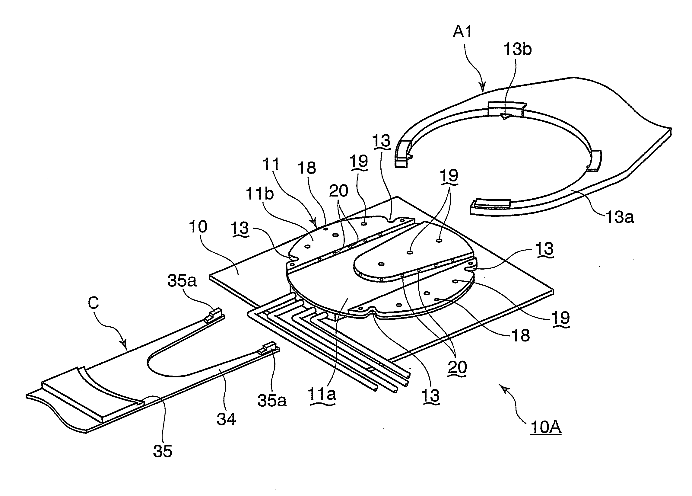
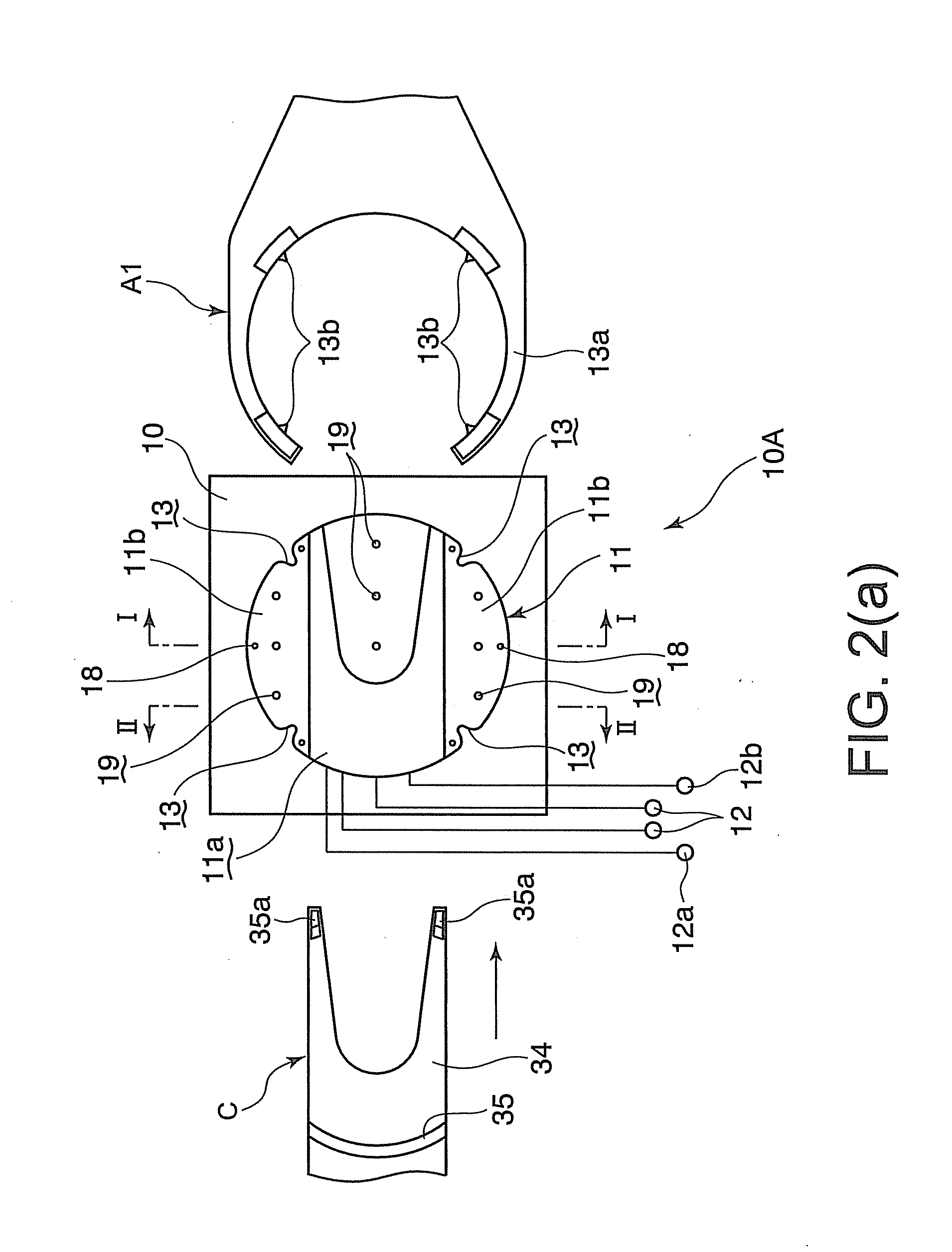
[0033]In the present invention, when a substrate is transported to a transport part with the use of two substrate transfer means of different shapes, it is not necessary, before a cooling process, to temporarily place the substrate on the substrate support pins which have been conventionally used during the transport operation. Thus, a reduction in throughput can be achieved. In addition, since the cooling surface sucks the substrate by the suction means, a time required for cooling the substrate can be reduced. Therefore, productivity of the overall apparatus can be improved.

Problems solved by technology

In this case, there are problems of heat accumulation in the cassette (FOUP) and / or warp of the wafer caused by a non-uniform temperature decrease in the cassette.

Method used


Image

  • Substrate processing apparatus
  • Substrate processing apparatus
  • Substrate processing apparatus

Examples


Embodiment Construction

[0046]An embodiment of the present invention will be described herebelow with reference to the attached drawings. Given herein as an example to describe the present invention is a case where a substrate processing apparatus according to the present invention is applied to a coating and developing apparatus for semiconductor wafers.

[0047]As shown in FIGS. 8 and 9, the coating and developing apparatus includes a carrier block S1 provided with a table 80a. From a carrier 80 which is a sealable-type substrate container placed on the table 80a, a transport arm C which is a second substrate transfer means takes out a wafer W and transports the wafer W to a processing block S2. Then, the transport arm C receives a processed wafer W from the processing block S2 and returns the wafer W to the carrier 80.

[0048]As shown in FIG. 8, the processing block S2 includes a first block (DEV layer) B1, a second block (BCT layer) B2, a third block (COT layer) B3, and a fourth block (TCT layer) B4, which ...


PUM


Abstract

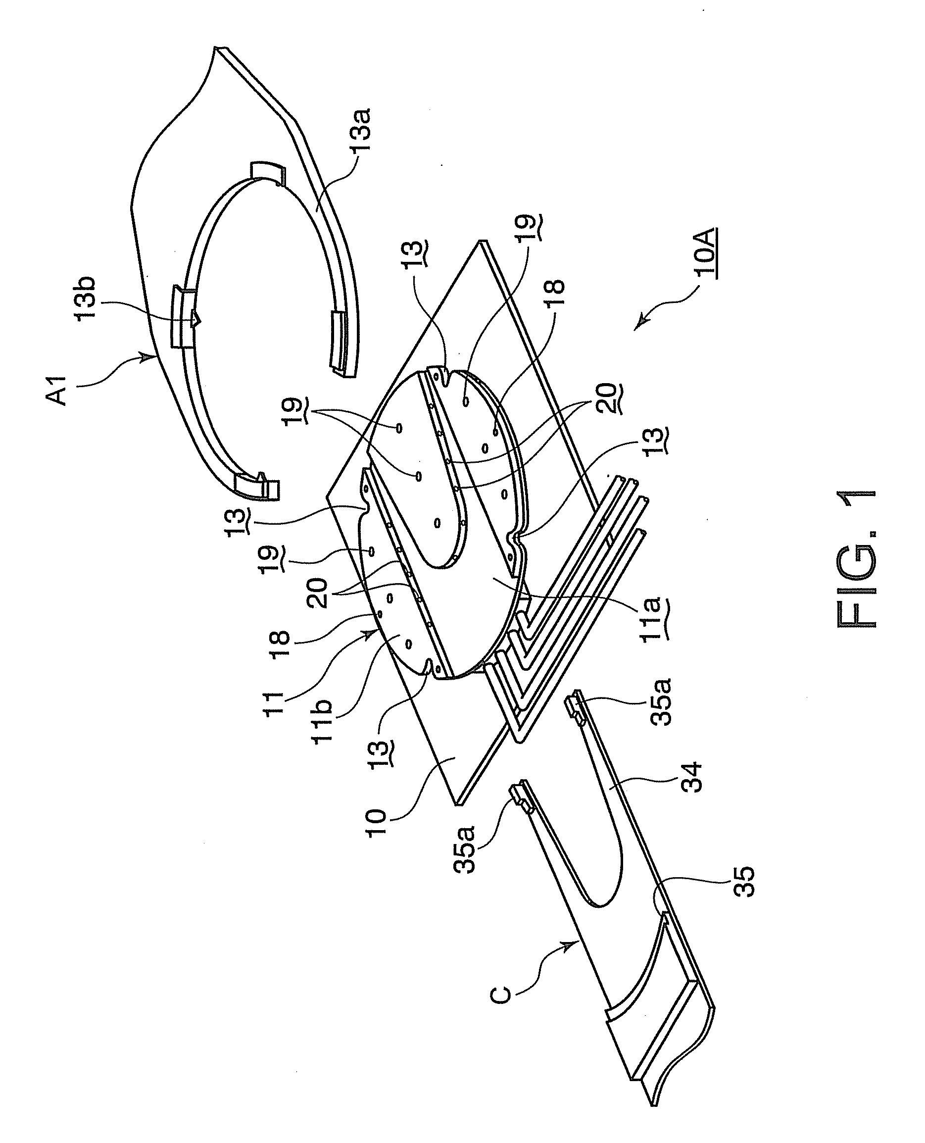
A substrate processing apparatus including: a heating part for heating a wafer; a transport part through which a wafer is transported; a first transfer arm that receives a wafer from the heating part and places the wafer on the transport part; and a second transfer arm including a pair of plate-like tweezers that receives the wafer placed on the transport part from the transport part and transfers the wafer. The transport part includes a cooling plate having a cooling surface on which a wafer is placed. The cooling plate includes a temperature-adjusting channel through which a temperature-adjusting water is circulated for cooling the cooling plate to a temperature lower than a temperature of the heating process of the heating part. The cooling surface is provided with a recess that is similar in shape to and slightly larger than a planar shape of the pair of tweezers.

Description

CROSS REFERENCE TO RELATED APPLICATIONS[0001]This application is based upon and claims the benefit of priority from the prior Japanese Patent Application No. 2009-025591 filed on Feb. 6, 2009, the entire contents of which are incorporated herein by reference.FIELD OF THE INVENTION[0002]The present invention relates to a processing apparatus for a substrate such as a semiconductor wafer and a glass substrate (FPD substrate) for liquid crystal display.BACKGROUND ART[0003]A step for forming a resist pattern on a substrate, which is one of processes for manufacturing a semiconductor device and an FPD substrate, is composed of a series of steps in which a resist film is formed on a substrate such as a semiconductor wafer (hereinafter referred to as “wafer”), the resist film is exposed with the use of a photomask, and thereafter a desired pattern is obtained by performing a developing process. These series of steps has been conventionally performed by a coating and developing apparatus.[0...

Claims


Application Information

Patent Timeline
Patent Type & Authority Applications(United States)
IPC IPC(8): B05C13/00G03B27/52
CPCH01L21/67109H01L21/68707H01L21/67748G06F1/20H05K7/20172
Inventor MIZUNAGA, KOUICHI
Owner TOKYO ELECTRON LTD
Why Eureka
Try Eureka