Methods of fabricating semiconductor devices and semiconductor devices including a contact plug processed by rapid thermal annealing

Active Publication Date: 2010-08-12
SAMSUNG ELECTRONICS CO LTD
View PDF8 Cites 59 Cited by
  • Summary
  • Abstract
  • Description
  • Claims
  • Application Information

AI Technical Summary

Benefits of technology

[0025]The method may include reducing the tungsten oxide (WξOψ) to pure tungsten (W) by performing rapid thermal hydrogenation (RTH) or rapid thermal ammoniation (RTNH) on the contact plug in a hydrogen or ammonia atmosph

Problems solved by technology

However, when the aspect ratio is high, it is difficult to ensure the step coverage of such an aluminum contact.
However, even when the HDPCVD method i

Method used


Image

  • Methods of fabricating semiconductor devices and semiconductor devices including a contact plug processed by rapid thermal annealing
  • Methods of fabricating semiconductor devices and semiconductor devices including a contact plug processed by rapid thermal annealing
  • Methods of fabricating semiconductor devices and semiconductor devices including a contact plug processed by rapid thermal annealing

Examples


Example

[0046]Korean Patent Application No. 10-2009-0011506, filed on Feb. 12, 2009, in the Korean Intellectual Property Office, and entitled: “Method of Fabricating Semiconductor Device,” is incorporated by reference herein in its entirety.

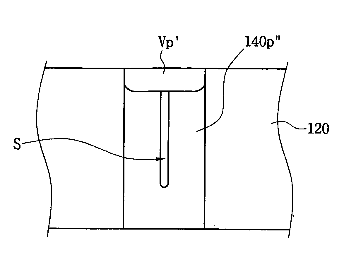
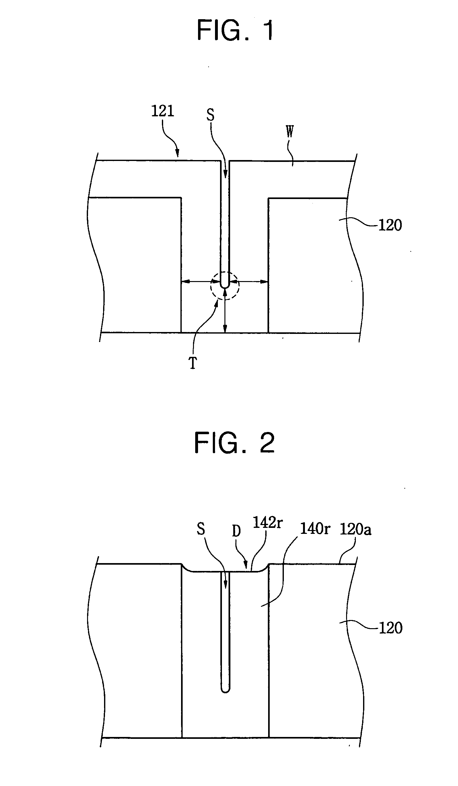
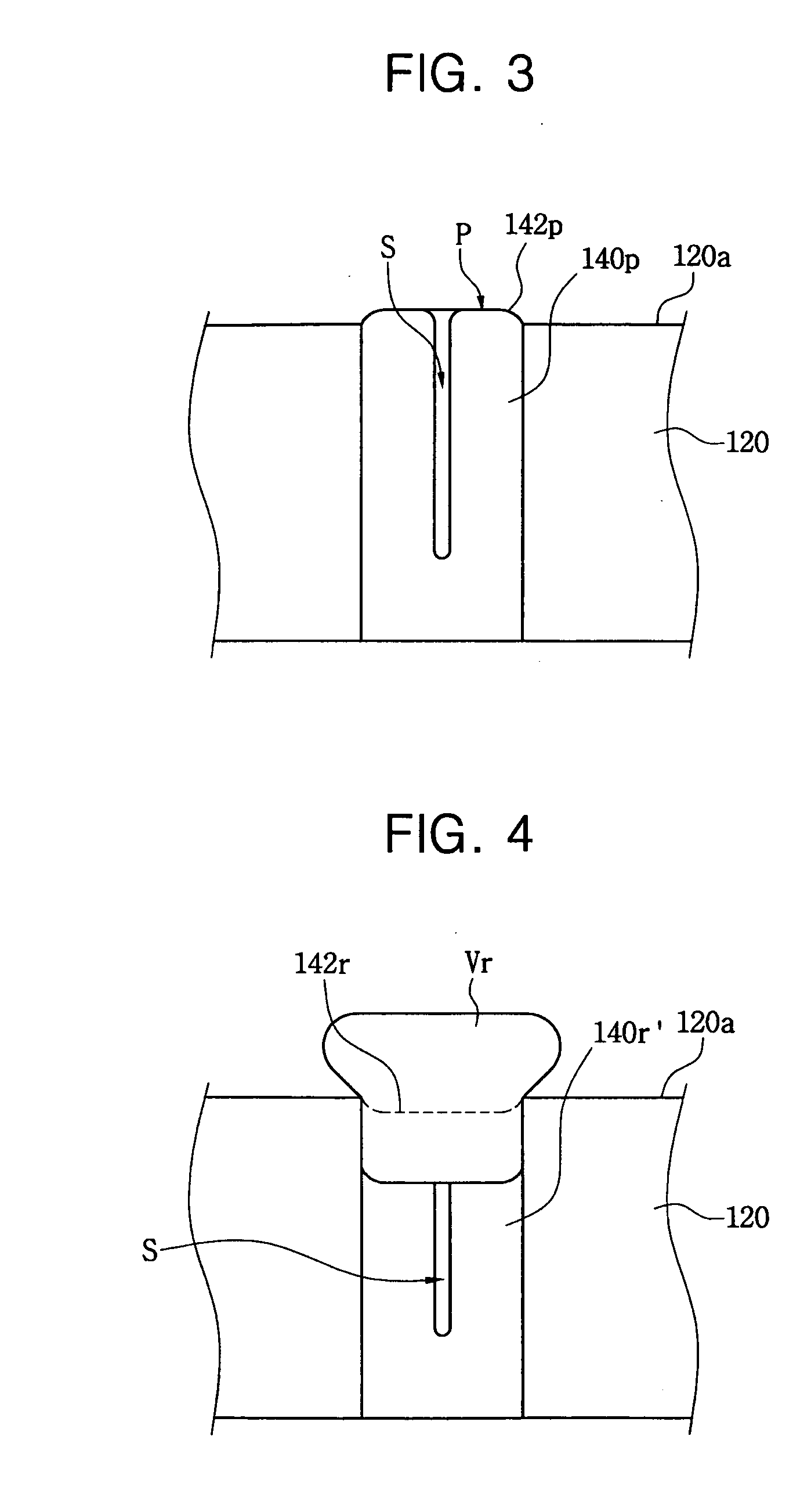
[0047]Various embodiments will now be described more fully with reference to the accompanying drawings in which some exemplary embodiments are shown. However, specific structural and functional details disclosed herein are merely representative for purposes of describing example embodiments. In the drawings, the thicknesses of layers and regions may be exaggerated for clarity. Further, it is understood that aspects may be embodied in many alternate forms and should not be construed as limited to only exemplary embodiments set forth herein. It will also be understood that when an element is referred to as being “on” another element, it can be directly on the other element, or intervening elements may also be present. Like reference numerals refer to like ...


PUM


Abstract

A method of fabricating a semiconductor device includes depositing tungsten on an insulating layer in which a contact hole is formed by chemical vapor deposition (CVD), performing chemical mechanical planarization (CMP) on the tungsten to expose the insulating layer and form a tungsten contact plug, and performing rapid thermal oxidation (RTO) on the tungsten contact plug in an oxygen atmosphere such that the tungsten expands volumetrically into tungsten oxide (WξOψ).

Description

BACKGROUND[0001]1. Field[0002]Embodiments relate to methods of fabricating semiconductor devices. More particularly, embodiments relate to methods of fabricating semiconductor devices in which a tungsten contact plug is processed by rapid thermal annealing (RTA) in an oxygen atmosphere to remove a partial step.[0003]2. Description of Related Art[0004]Today's rapidly developing information-oriented society demands semiconductor devices having high data transmission rates that can rapidly process large amounts of information. To increase the data transmission rate of a semiconductor device, design rules of semiconductor devices are being gradually reduced in order to integrate more and more cells on each single chip.[0005]That is, to form more and more patterns on a semiconductor substrate, pattern intervals and widths are being reduced. Patterns having a narrow width may be formed in multiple layers, and an interlayer insulating layer is formed to electrically insulate the patterns i...

Claims


Application Information

Patent Timeline
IPC IPC(8): H01L21/768
CPCH01L21/321H01L21/3212H01L21/76883H01L21/76877H01L21/7684A61G17/04
Inventor CHOI, SUK-HUNHONG, CHANG-KICHOI, JAE-HYOUNGSON, YOON-HOPARK, MIN-YOUNGTAK, YONG-SUK
Owner SAMSUNG ELECTRONICS CO LTD
Why Eureka
Try Eureka