

Semiconductor wafer metrology apparatus and method
a technology of semiconductor wafers and metrology equipment, applied in the field of semiconductor wafer metrology, can solve the problems of change in the mass at or on the surface of semiconductor wafers, errors may be caused, and need to be taken into account, so as to reduce the weight error force and reduce the error
- Summary
- Abstract
- Description
- Claims
- Application Information
AI Technical Summary
Benefits of technology
Problems solved by technology
Method used
Image

Examples
Embodiment Construction
; FURTHER OPTIONS AND PREFERENCES
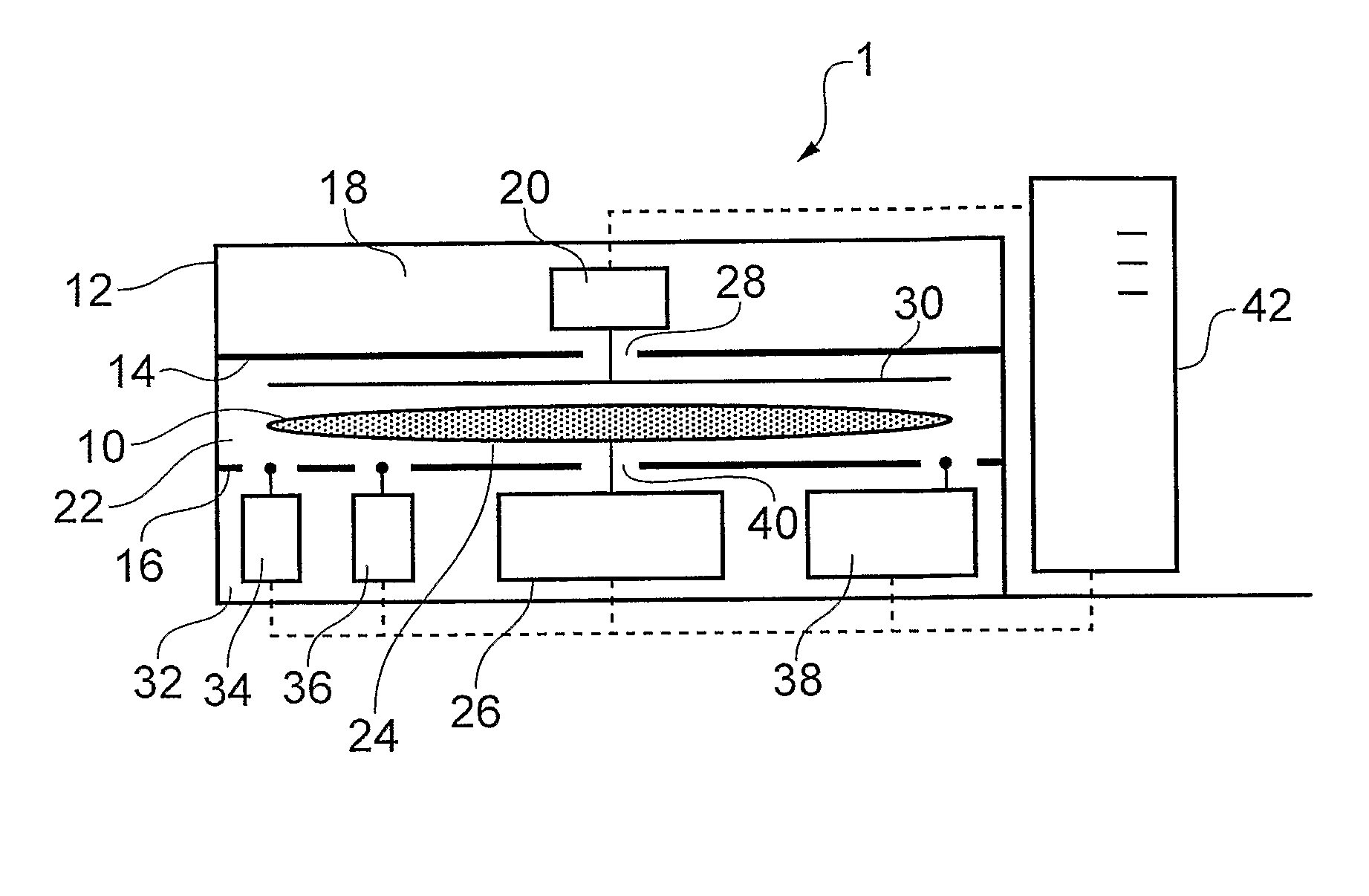
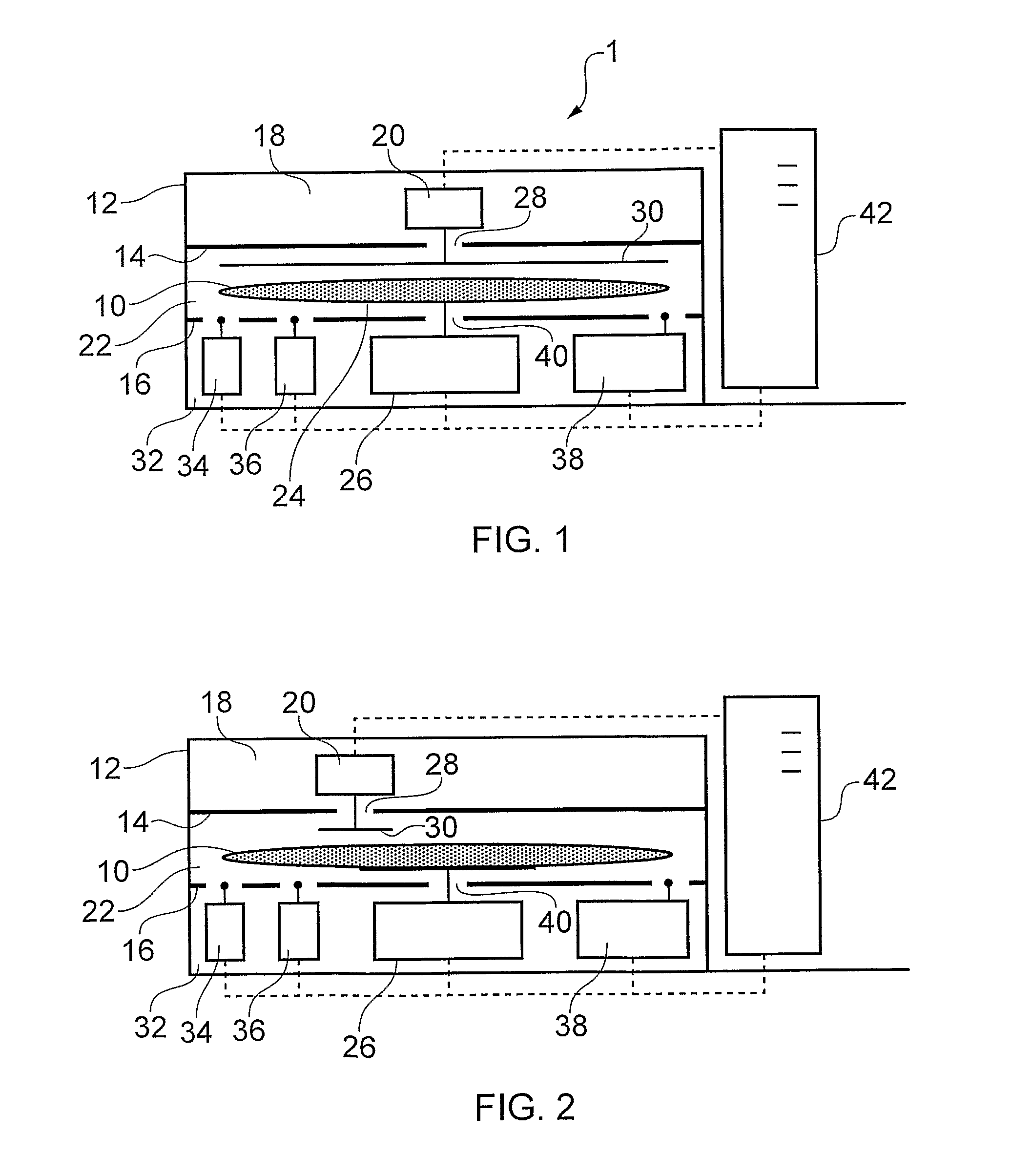
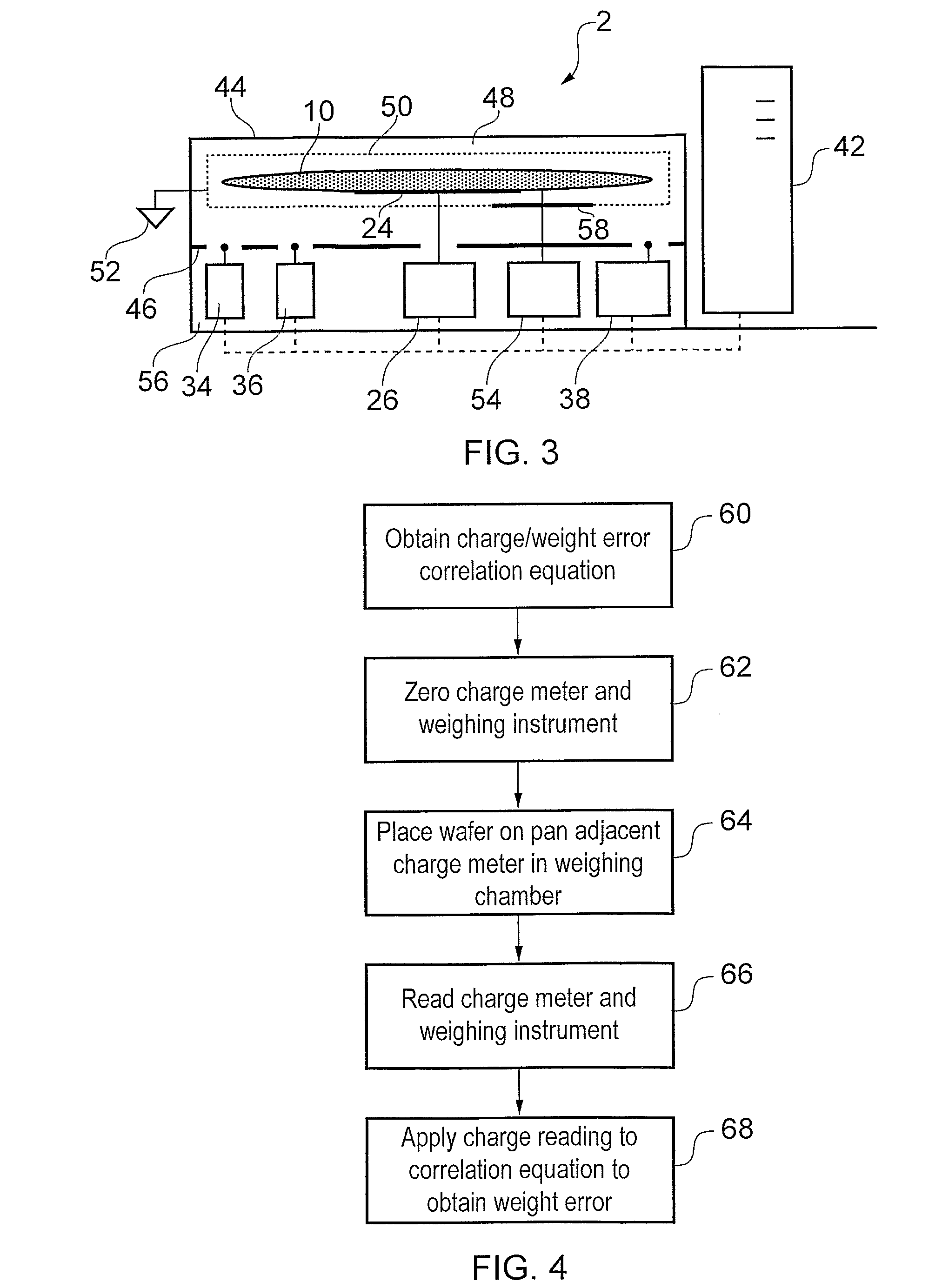
[0039]FIG. 1 shows weighing apparatus 1 which includes a chamber 12 arranged to enclose a semiconductor wafer 10 and various measuring instruments (discussed below) during a weight measurement. The chamber 12 encloses the system in part to prevent or reduce the effect of air currents in causing errors in the weight measurement.
[0040]In FIG. 1, the chamber 12 is partitioned into three portions by partition walls 14, 16. An upper portion 18 contains a charge meter 20, e.g. a Trifield Electrostatic Voltmeter. A middle portion 22 is sized to receive the wafer 10 and also includes the pan 24 of a weighing instrument 26, e.g. a suitable microbalance having 0.01 mg resolution and less than 0.03 mg repeatability (e.g. a Sartorius WZA225-CW). The chamber 12 includes a door (not shown) into the middle portion 22 for deliver and removal of the wafer 10. The partition wall 14 separating the upper and middle portions includes a through hole 28, which allows a sen...
PUM
 Abstract
Description
Claims
Application Information