Semiconductor device including a transistor, and manufacturing method of the semiconductor device

a semiconductor device and semiconductor technology, applied in the direction of transistors, electroluminescent light sources, electric lighting sources, etc., can solve the problems of deterioration of electrical characteristics of elements, problems of variation, and likely variation of semiconductor characteristics, so as to suppress the deterioration of electrical characteristics of transistors

Active Publication Date: 2010-08-19
SEMICON ENERGY LAB CO LTD
View PDF38 Cites 45 Cited by
  • Summary
  • Abstract
  • Description
  • Claims
  • Application Information

AI Technical Summary

Benefits of technology

[0033]According to an embodiment of the present invention, a p-type silicon layer is provided over and in contact with a surface of an oxide semiconductor layer i...

Problems solved by technology

However, semiconductor characteristics are likely to vary because of damage to the oxide semiconductor due to an etchant or plasma or contamination of an element such as hy...

Method used


Image

  • Semiconductor device including a transistor, and manufacturing method of the semiconductor device
  • Semiconductor device including a transistor, and manufacturing method of the semiconductor device
  • Semiconductor device including a transistor, and manufacturing method of the semiconductor device

Examples


embodiment 1

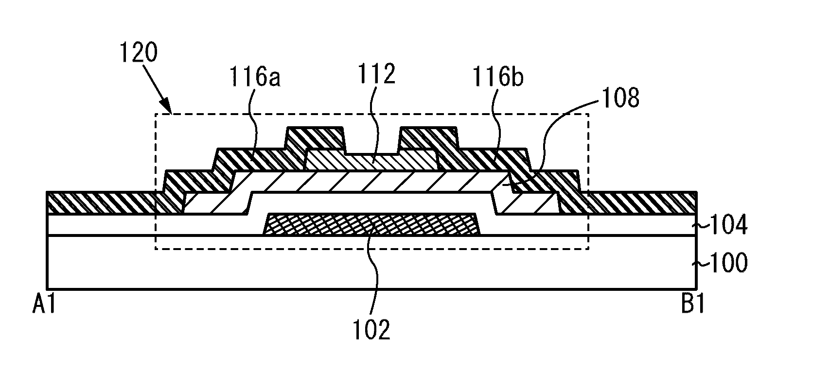
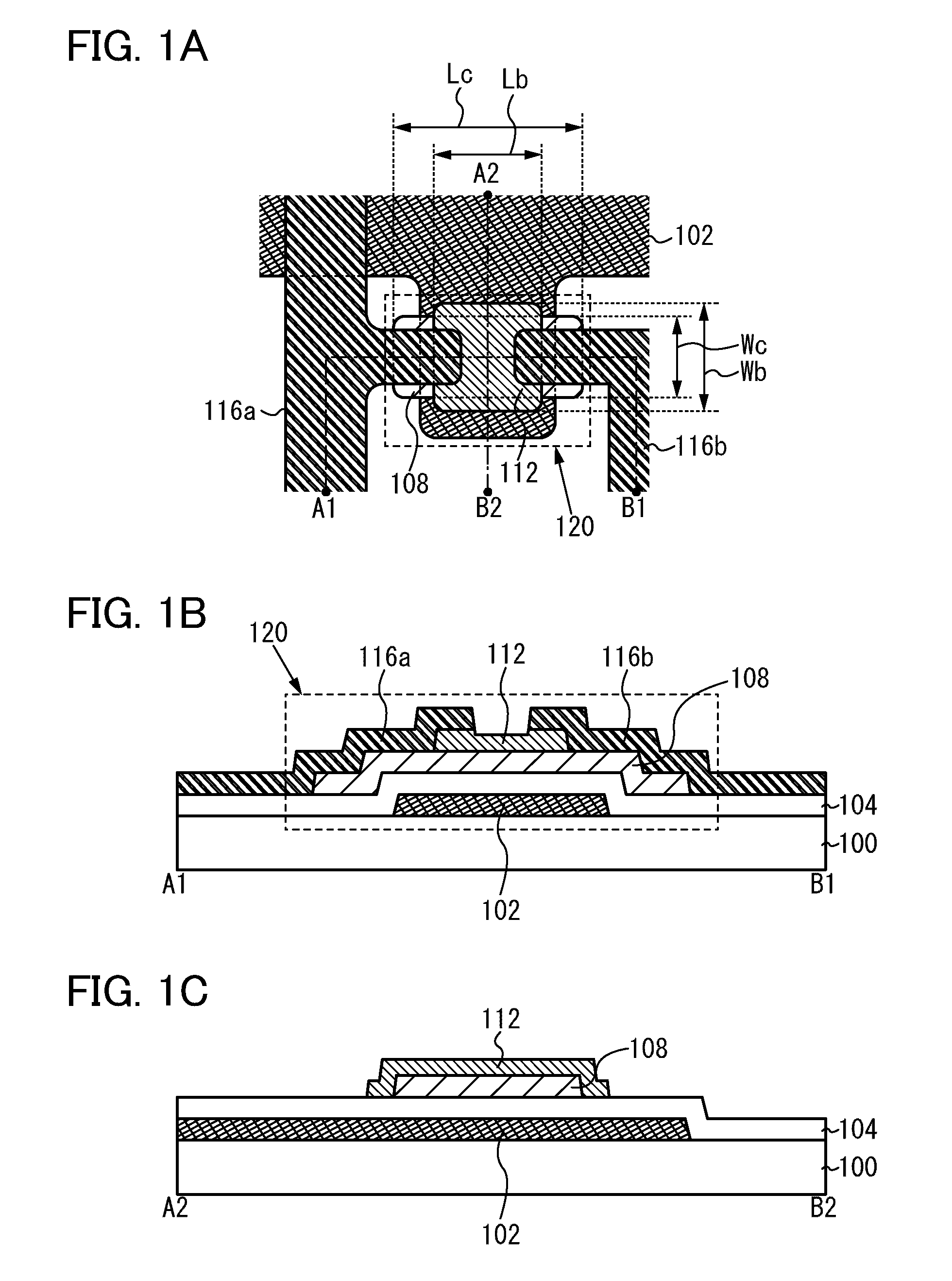
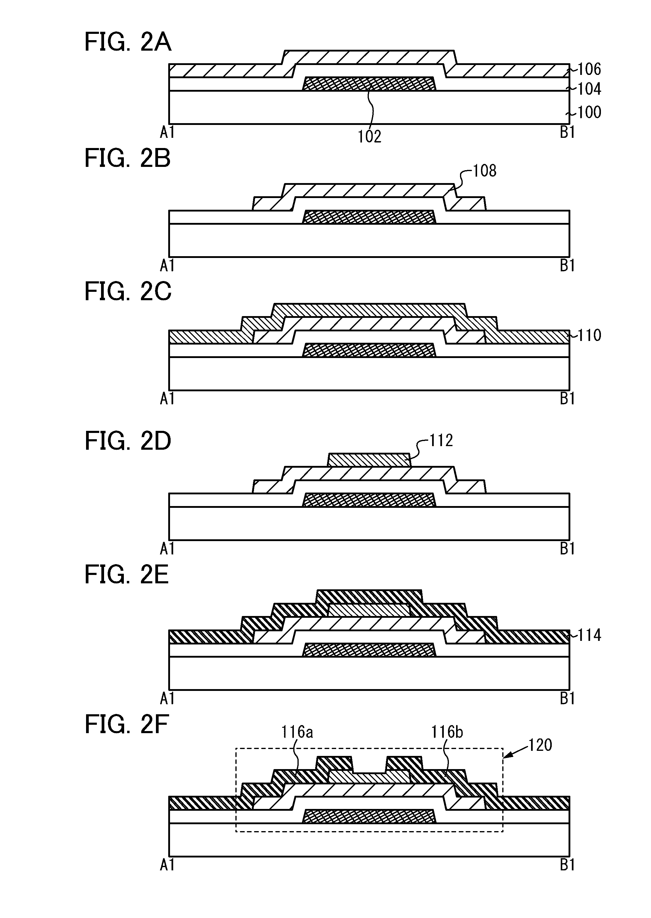
[0068]In this embodiment, an example of a structure of a transistor included in a semiconductor device will be described with reference to drawings.

[0069]A transistor 120 illustrated in FIGS. 1A to 1C includes a gate (including a gate wiring and a gate electrode (hereinafter referred to as a “gate electrode 102”)) provided over a substrate 100, a gate insulating layer 104 provided over the gate electrode 102, an oxide semiconductor layer 108 provided over the gate insulating layer 104, a p-type silicon layer 112 provided over and in contact with a surface of the oxide semiconductor layer 108, and a source (including a source wiring and a source electrode (hereinafter referred to as a “source electrode layer 116a”)) and a drain (including a drain wiring and a drain electrode (also referred to as a “drain electrode layer 116b”)) which are electrically connected to the oxide semiconductor layer 108 (see FIGS. 1A to 1C).

[0070]FIG. 1A is a top view, FIG. 1B is a cross-sectional view take...

embodiment 2

[0160]In this embodiment, a structure and a manufacturing method of a transistor which is different from that of Embodiment 1 will be described with reference to drawings.

[0161]First, the manufacturing method of the transistor will be described with reference to FIGS. 5A to 5E. Note that the manufacturing process (such as applicable materials) described in this embodiment is in common with that of Embodiment 1 in many points. Thus, description of the common points is omitted below and only points different from those of Embodiment 1 will be described in detail.

[0162]First, the gate electrode 102 is formed over the substrate 100, and then the gate insulating layer 104 is formed over the gate electrode 102. Then, the oxide semiconductor layer 106 and the p-type silicon layer 110 are sequentially formed to be stacked over the gate insulating layer 104, and a resist mask 171 is selectively formed (see FIG. 5A). It is preferable that layers of from the gate insulating layer 104 to the p-...

embodiment 3

[0174]In this embodiment, a transistor which is different from the transistors in Embodiments 1 and 2 and a manufacturing method thereof will be described with reference to drawings. Note that the manufacturing process (such as applicable materials) described in this embodiment is in common with that of Embodiment 1 in many points. Thus, description of the common points is omitted below and only points different from those of Embodiment 1 will be described in detail.

[0175]A transistor 140 illustrated in FIGS. 7A and 7B includes the gate electrode 102 provided over the substrate 100, the gate insulating layer 104 provided over the gate electrode 102, the oxide semiconductor layer 108 provided over the gate insulating layer 104, the p-type silicon layer 112 provided over and in contact with the surface of the oxide semiconductor layer 108, and the source electrode layer 116a and the drain electrode layer 116b provided over and in contact with the surface of the oxide semiconductor lay...


PUM


Abstract

The object is to suppress deterioration in electrical characteristics in a semiconductor device comprising a transistor including an oxide semiconductor layer. In a transistor in which a channel layer is formed using an oxide semiconductor, a p-type silicon layer is provided in contact with a surface of the oxide semiconductor layer. Further, the p-type silicon layer is provided in contact with at least a region of the oxide semiconductor layer, in which a channel is formed, and a source electrode layer and a drain electrode layer are provided in contact with regions of the oxide semiconductor layer, over which the p-type silicon layer is not provided.

Description

BACKGROUND OF THE INVENTION[0001]1. Field of the Invention[0002]The present invention relates to a transistor that uses an oxide semiconductor layer, a semiconductor device including the transistor, and a manufacturing method of the transistor and the semiconductor device.[0003]2. Description of the Related Art[0004]There are various kinds of metal oxides, which are used for a wide range of applications. Indium oxide is a well-known material and used as a material of a transparent electrode which is needed in a liquid crystal display or the like.[0005]Some metal oxides exhibit semiconductor characteristics. In general, metal oxides serve as insulators; however, it is known that metal oxides can serve as semiconductors depending on the combination of elements included in the metal oxides.[0006]For example, tungsten oxide, tin oxide, indium oxide, zinc oxide, and the like can be given as metal oxides exhibiting semiconductor characteristics, and thin film transistors in which a channe...

Claims


Application Information

Patent Timeline
IPC IPC(8): H01L29/786H01L21/34H05B44/00
CPCH01L21/02554H01L21/02565H01L29/7869H01L27/1225H01L21/02631H01L29/78606
Inventor SAKATA, JUNICHIROGODO, HIROMICHISHIMAZU, TAKASHI
Owner SEMICON ENERGY LAB CO LTD
Why Eureka
Try Eureka