Process for manufacturing circuit board and circuit board

Inactive Publication Date: 2010-08-26
SUMITOMO BAKELITE CO LTD
View PDF7 Cites 7 Cited by
  • Summary
  • Abstract
  • Description
  • Claims
  • Application Information

AI Technical Summary

Benefits of technology

[0017]The present invention includes the steps under the predetermined conditions optimal for removing the interlayer adhesive, forming the fillet and form

Problems solved by technology

However, the above method may not provide adequately reliable interlayer electric connection because the connection is formed via a conductive adhesive.
Furthermore, the method requires an advanced technique for filling a fine via hole with a conductive adhesive and thus cannot cope with further miniaturization of an interconnection pattern.
However, this method cannot completely remove the interlayer adhesive between the conductor post and

Method used


Image

  • Process for manufacturing circuit board and circuit board
  • Process for manufacturing circuit board and circuit board
  • Process for manufacturing circuit board and circuit board

Examples


example 1

Preparation of an Interlayer Adhesive

[0123]Forty parts by weight of a bisphenol-A type epoxy resin (Dainippon Ink And Chemicals, Incorporated, EPICLON 840-S), 20 parts by weight of a novolac type phenol resin (Sumitomo Bakelite Co., Ltd., PR-53647), 20 parts by weight of a phenoxy resin (Japan Epoxy Resins Co., Ltd., YL-6954, number average molecular weight: 14500), 20 parts by weight of phenolphthaline (Kanto Chemical Co., Inc., Reagent grade) and 100 parts by weight of acetone were weighed, and mixed and stirred to give an interlayer adhesive. This interlayer adhesive was measured for a copper-oxide reduction rate, a solder wet spread rate and a melt viscosity as described above and the following results were obtained.

[0124]Copper-oxide reduction rate: 85%

[0125]Solder wet spread rate:

[0126]Solder ball[0127]SnPt: 55%[0128]SnAgCu: 52%[0129]SnBi: 54%

[0130]Melt viscosity: 1000 Pa·s

Preparation of a Circuit Board

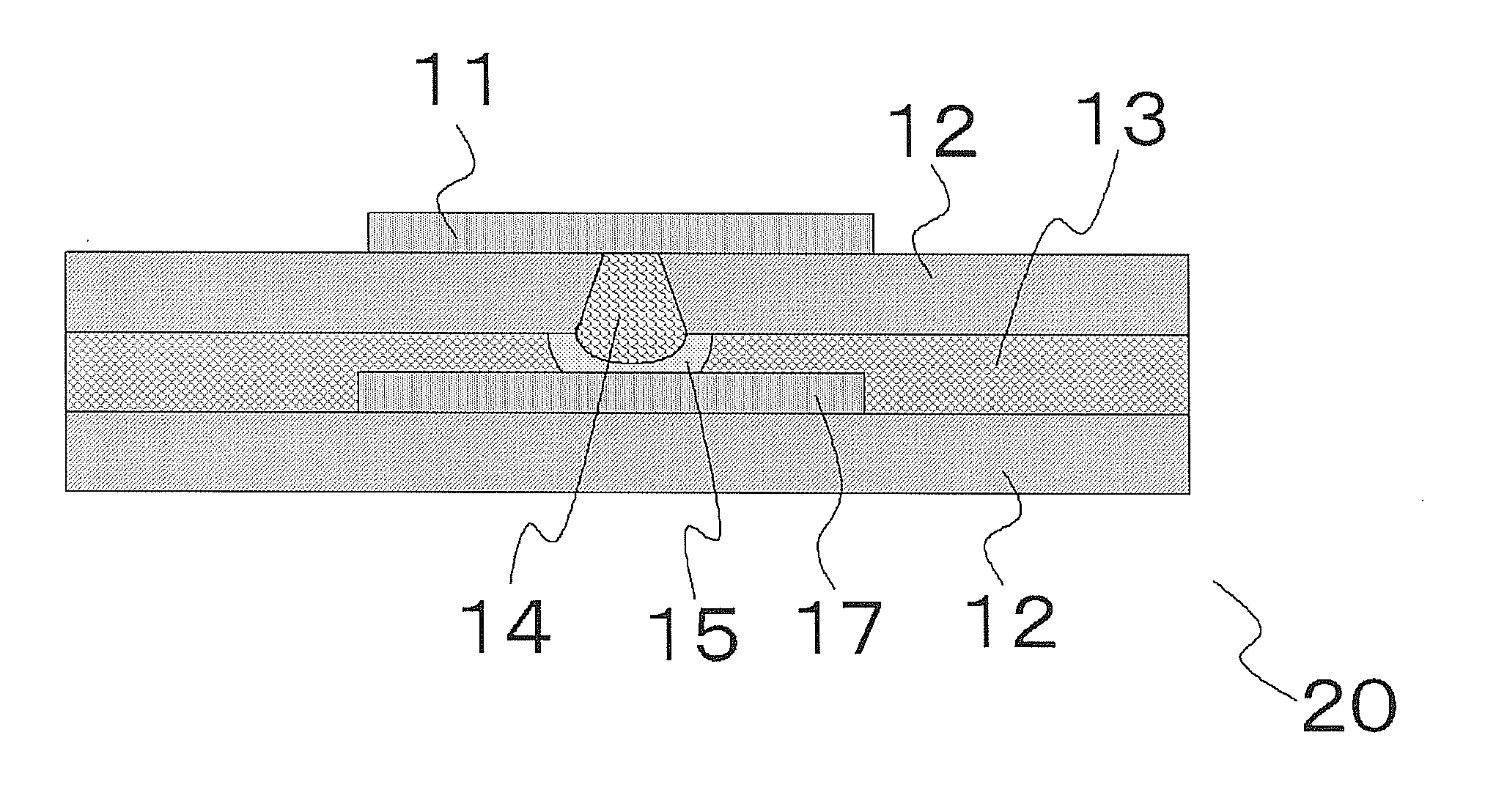
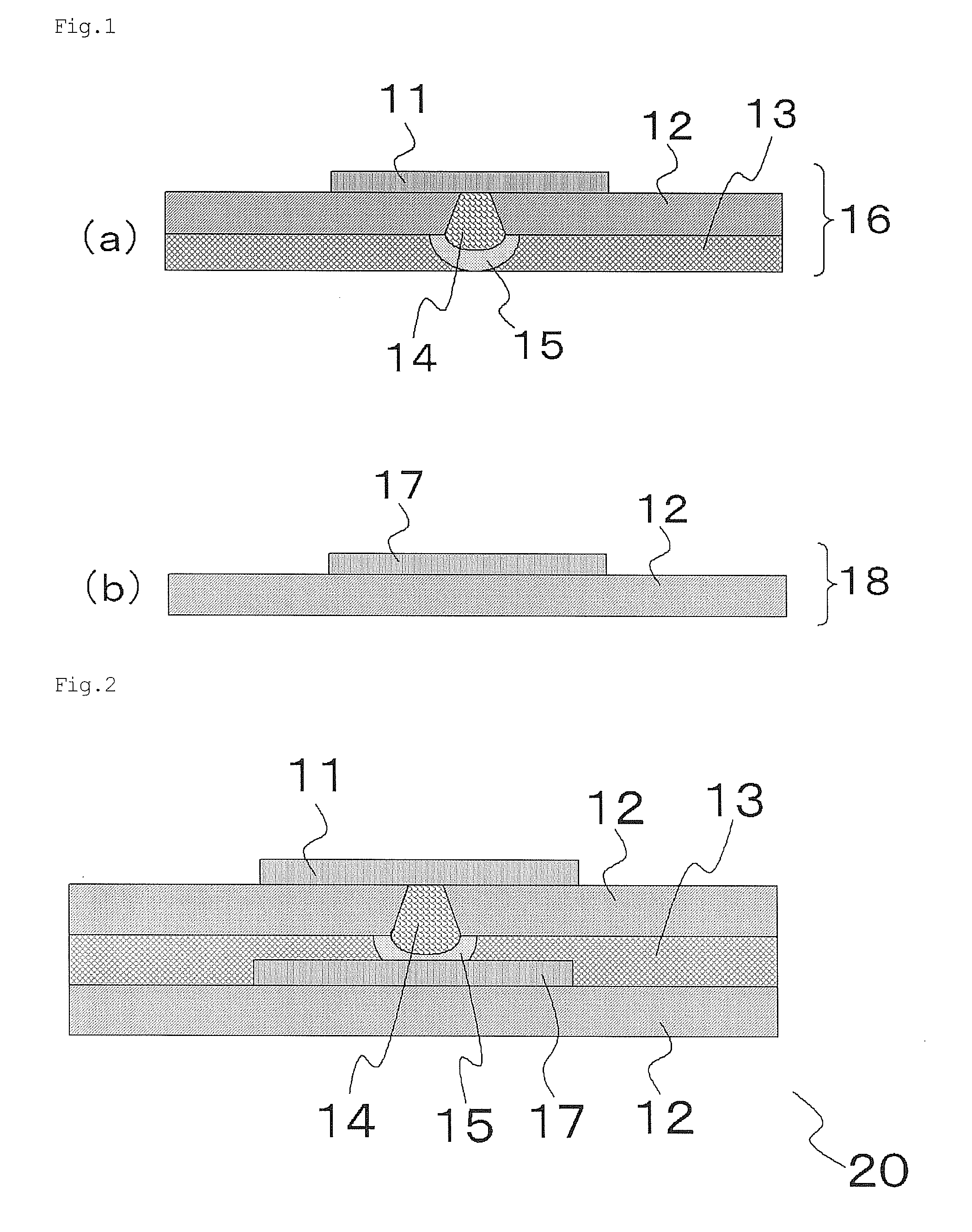
[0131]A circuit board was prepared in accordance with the steps illustrated...

example 2

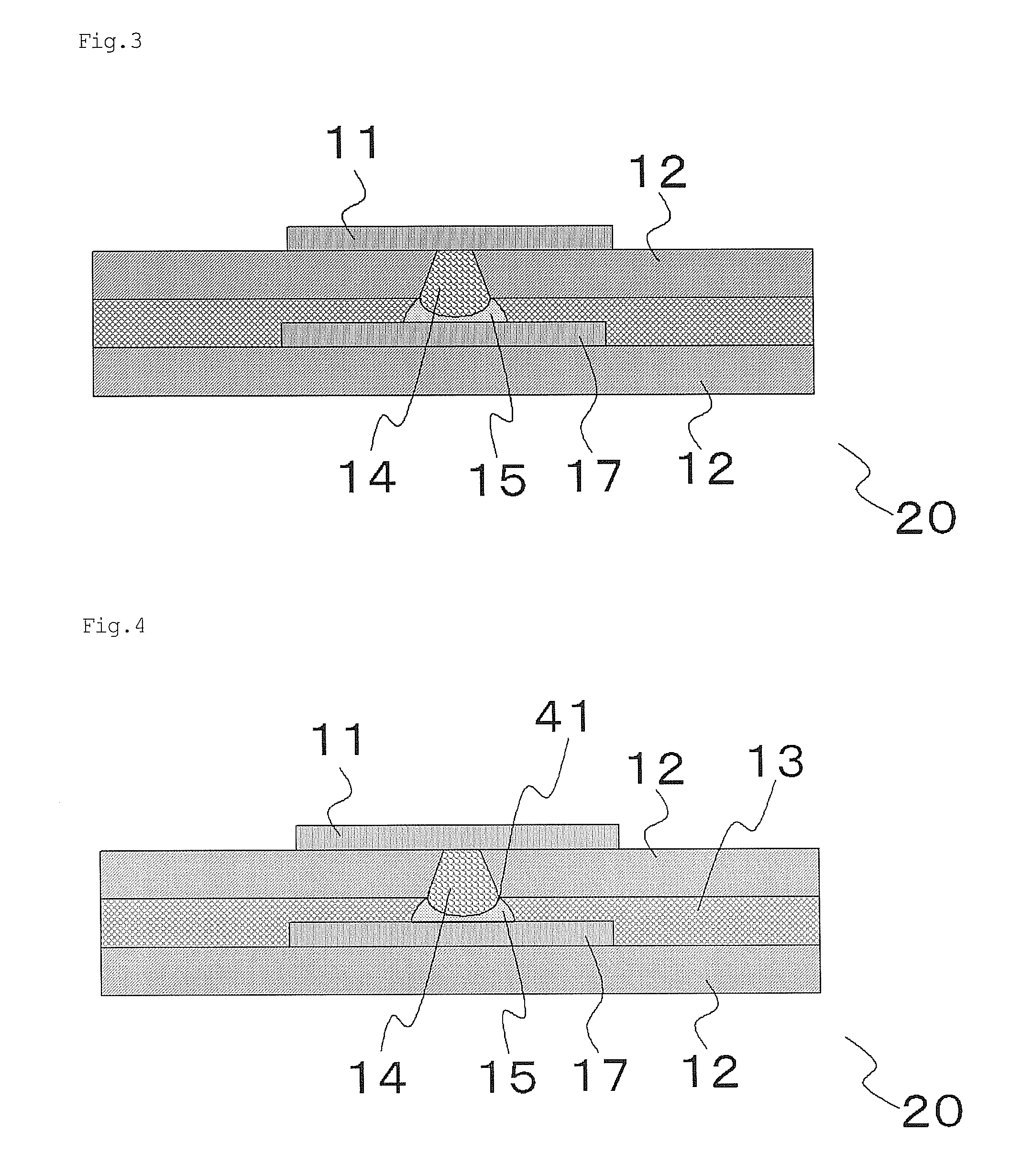
[0133]A circuit board was prepared as described in Example 1, except thermocompression was conducted at 220° C. and 2 MPa and pressing was conducted at 221° C. and 1 MPa for 25 sec.


PUM

PropertyMeasurementUnit
Temperatureaaaaaaaaaa

Abstract

According to the present invention, there is provided a process for manufacturing a circuit board wherein a first substrate having a conductor post and a second substrate having a conductor pad for receiving the conductor post are laminated through an interlayer adhesive, and the conductor post and the conductor pad are electrically connected, comprising, as a first step, bonding the conductor pad with the conductor post by thermocompression under predetermined first conditions while the first and the second substrates are arranged such that the conductor pad faces the conductor post through the interlayer adhesive; thermocompressing the first substrate and the second substrate under predetermined second conditions while the conductor pad is bonded with the conductor post; and thermocompressing the first substrate and the second substrate under predetermined third conditions while the conductor pad is bonded with the conductor post, wherein the first, the second and the third conditions are different from each other.

Description

TECHNICAL FIELD[0001]The present invention relates to a process for manufacturing a circuit board and a circuit board.BACKGROUND ART[0002]Recent density increase in electronic devices has accelerated multilayering of a circuit board used in these devices such as a flexible printed circuit board. A build-up method is generally employed for laminating such a multilayer circuit board. A build-up method refers to a method for forming interlayer connection between monolayers while piling up resin layers made of a resin alone and conductor layers.[0003]The build-up methods can be generally categorized into those where a via hole is formed in resin layers before forming an interlayer connection and those where an interlayer connection is formed before laminating resin layers. Methods for forming an interlayer connection are categorized into formation of a via hole by plating and formation using a conductive paste.[0004]There has been disclosed a technique allowing for stacked-via and densi...

Claims


Application Information

Patent Timeline
IPC IPC(8): H05K1/00H05K13/00
CPCH05K3/3489H05K3/386H05K3/423H05K3/4617H05K2201/0195H05K2201/0394Y10T29/49126H05K2203/0733Y10T29/49117Y10T29/49156Y10T29/49165Y10T29/4913H05K2203/068H05K3/46
Inventor KONDO, MASAYOSHIKOMIYATANI, TOSHIO
Owner SUMITOMO BAKELITE CO LTD
Why Eureka
Try Eureka