Gallium nitride-based semiconductor optical device, method of fabricating gallium nitride-based semiconductor optical device, and epitaxial wafer

a semiconductor optical device and gallium nitride technology, applied in semiconductor devices, lasers, semiconductor lasers, etc., can solve the problem of not providing any appropriate cleavage plane, and achieve the effect of low piezoelectric effect and high crystal quality

Inactive Publication Date: 2010-09-02
SUMITOMO ELECTRIC IND LTD
View PDF6 Cites 14 Cited by
  • Summary
  • Abstract
  • Description
  • Claims
  • Application Information

AI Technical Summary

Benefits of technology

[0047]As described above, one aspect of the present invention provides a gallium nitride-based semiconductor optical device including an indium-containing gallium nitride-based semiconductor layer that exhibits low piezoelectric effect and high crystal quality. Besides...

Problems solved by technology

However, the above inclination to the c-axi...

Method used


Image

  • Gallium nitride-based semiconductor optical device, method of fabricating gallium nitride-based semiconductor optical device, and epitaxial wafer
  • Gallium nitride-based semiconductor optical device, method of fabricating gallium nitride-based semiconductor optical device, and epitaxial wafer
  • Gallium nitride-based semiconductor optical device, method of fabricating gallium nitride-based semiconductor optical device, and epitaxial wafer

Examples


example 1

Light-Emitting Diode

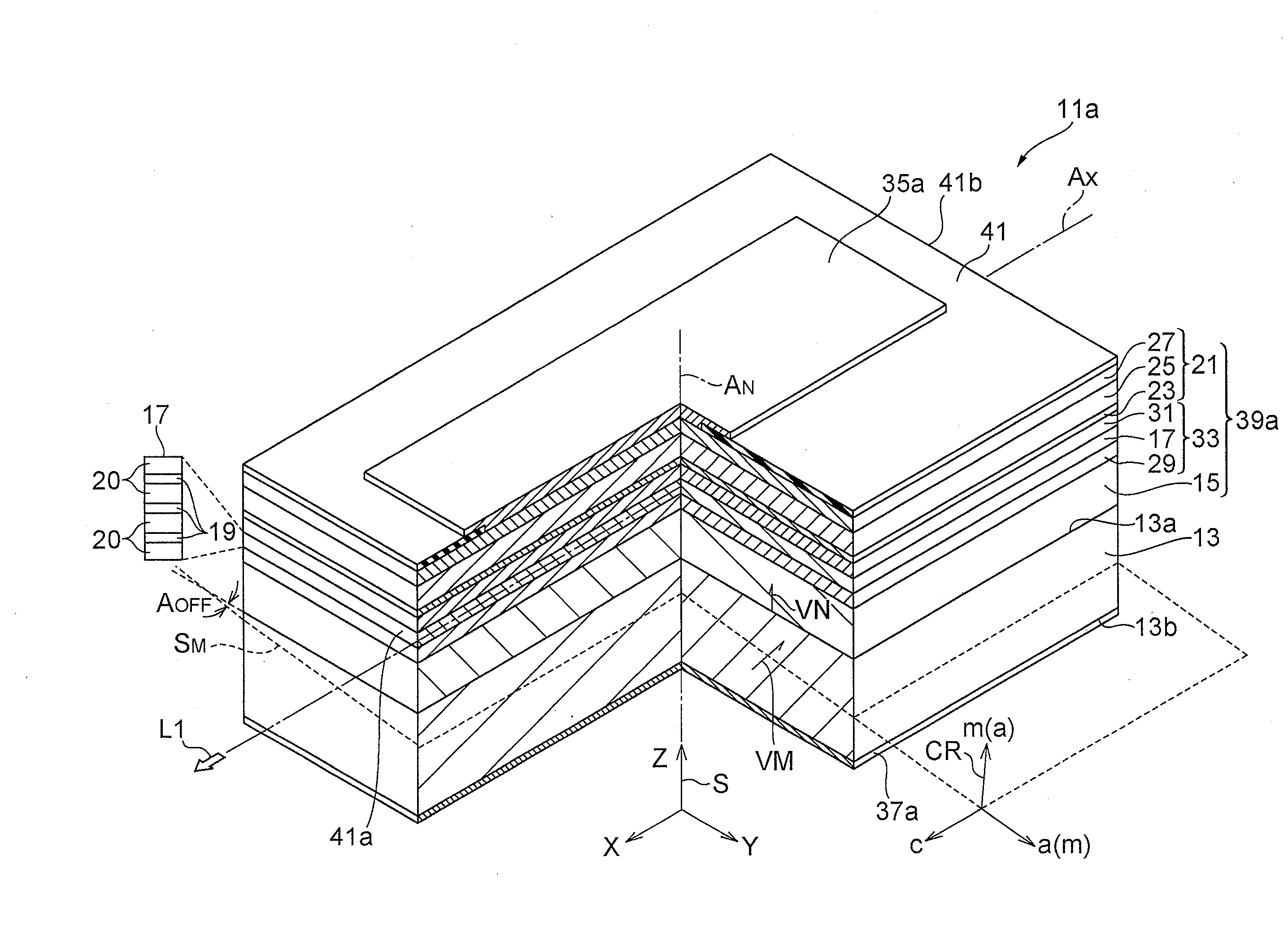
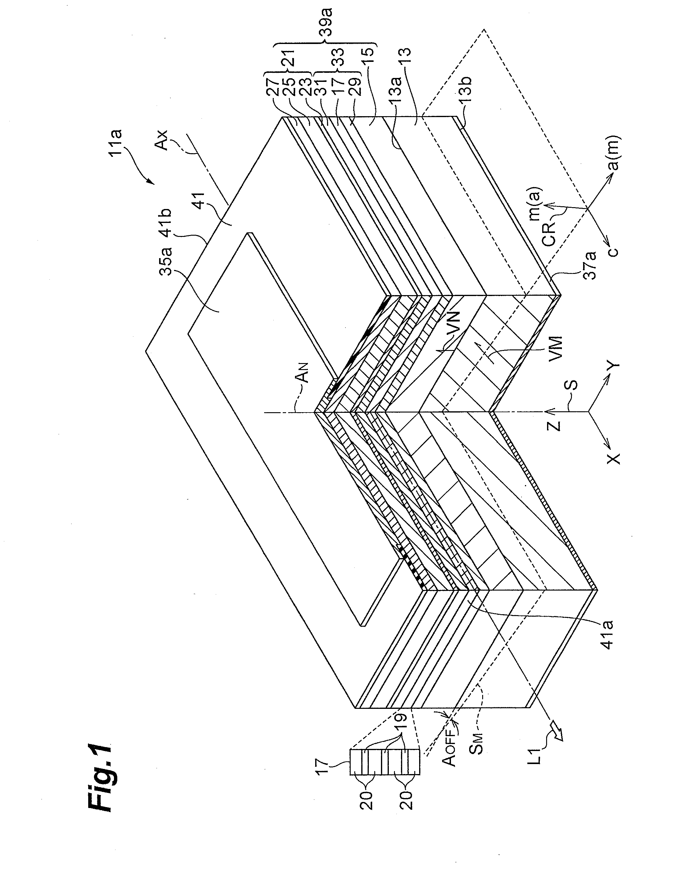
[0082]In Example 1, a light-emitting diode shown in FIG. 4 was fabricated. A number of gallium nitride-based wafers were prepared, and these wafers have the primary surfaces that tilt by a specified angle θA with reference to the m-axis of hexagonal GaN from the m-plane toward the a-axis of hexagonal GaN. The tilt angle θA was in the range of zero to 0.12 degree. The off angle θC of each of the substrates was 0.6 degree in terms of the c-axis of the substrates. A light-emitting diode structure was fabricated on each wafer by organometallic vapor phase epitaxy. The following raw materials were used: trimethyl-gallium (TMG), trimethyl-aluminum (TMA), trimethyl-indium (TM), ammonia (NH3), silane (SiH4), and bis(cyclopentadienyl)magnesium (CP2Mg).

[0083]All GaN wafers were loaded on a susceptor in the reactor, and then NH3 and H2 were supplied thereto to heat-treat them at a temperature of 1050° C. and under a reactor pressure of 27 kPa. The period of the heat treatme...

example 2

Light-Emitting Diode

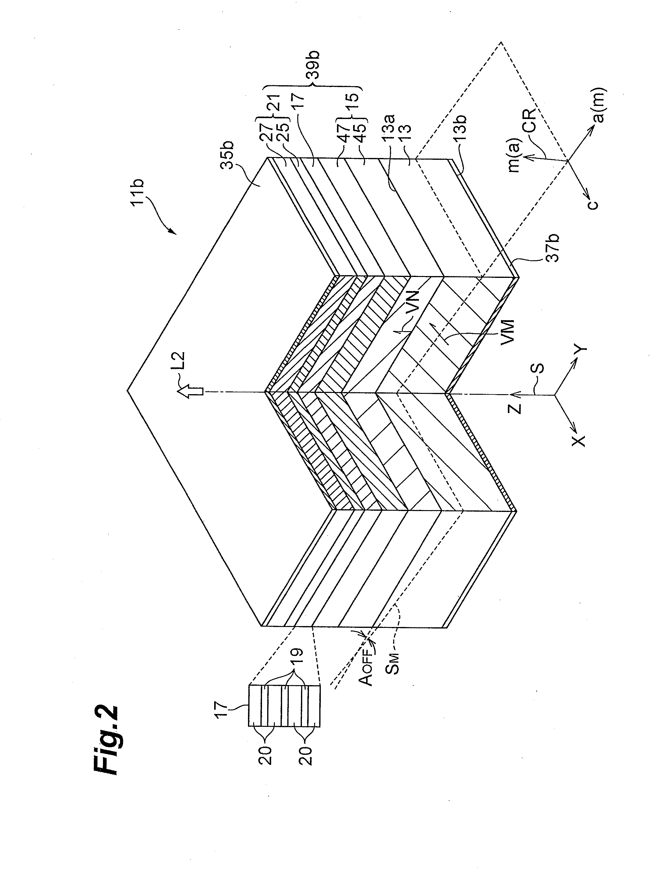
[0092]Four GaN wafers, which are referred to as Ma, M0, M1, and C, were prepared. In the GaN wafer Ma, the m-plane of hexagonal GaN tilted by an off angle of 0.1 degree in the direction from the m-plane toward the a-axis, and the primary surface of the GaN wafer Ma tilts with reference to the m-plane by an off angle of 0.1 degree. Each of the GaN wafers M0 and M1 had a primary surface of the just m-plane. The GaN wafer C had a primary surface of the just c-plane. Light-emitting diode structures were fabricated on the primary surface of these GaN wafers by organometallic vapor phase epitaxy. Raw materials used in the growth were the same as those used in Example 1.

[0093]The GaN wafers Ma, M0, and C were loaded on a susceptor in the reactor, and then NH3 and H2 were supplied thereto to heat-treat them at a temperature of 1050° C. and under a reactor pressure of 27 kPa for 10 minutes. After that, a Si-doped GaN layer having a thickness of 2000 nanometers was grown a...

example 3

Semiconductor Laser

[0101]A GaN wafer was prepared. In this GaN wafer, an m-plane of hexagonal GaN tilted by an off angle of 0.1 degree in a direction from the m-axis toward the a-axis, and accordingly the GaN wafer had the primary surface tilted by an off angle of 0.1 degree with reference to the m-plane.

[0102]After heat treating the surface of the GaN wafer, an n-type AlGaN cladding layer was grown at a wafer temperature of 1150° C. A lower optical confinement layer, an active layer, and an upper optical confinement layer were grown on the n-type AlGaN cladding layer at a wafer temperature of 840° C. A p-type AlGaN electron-blocking layer was grown on the upper optical confinement layer, and then a p-type GaN contact layer was grown on the p-type AlGaN electron-blocking layer at a wafer temperature of 1000° C. After an insulating film, such as a silicon film, was formed on the p-type GaN contact layer, a stripe window of 10 μm wide was formed in the insulating film by photolithogra...


PUM


Abstract

A gallium nitride-based semiconductor optical device is provided that includes an indium-containing gallium nitride-based semiconductor layer that exhibit low piezoelectric effect and high crystal quality. The gallium nitride-based semiconductor optical device 11a includes a GaN support base 13, a GaN-based semiconductor region 15, and well layers 19. A primary surface 13a tilts from a surface orthogonal to a reference axis that extends in a direction from one crystal axis of the m-axis and the a-axis of GaN toward the other crystal axis. The tilt angle AOFF is equal to the angle defined by a vector VM and a vector VN. The inclination of the primary surface is shown by a typical m-plane SM and m-axis vector VM. The GaN-based semiconductor region 15 is provided on the primary surface 13a. In the well layers 19 in an active layer 17, both the m-plane and the a-plane of the well layers 19 tilt from a normal axis AN of the primary surface 13a. The indium content of the well layers 19 is 0.1 or more.

Description

TECHNICAL FIELD[0001]The present invention relates to a gallium nitride-based semiconductor optical device, a method of fabricating a gallium nitride-based semiconductor optical device, and an epitaxial wafer.BACKGROUND ART[0002]Nonpatent Literature 1 discloses a GaN-based light-emitting diode. The GaN-based light-emitting diode is formed on an m-plane GaN substrate. The surface morphology of an n-type GaN layer is improved by an increase in off angle defined in the direction from an m-axis to a c-axis. Nonpatent literature 2 discloses hillocks on an m-plane of an n-type GaN film.[0003]Patent Literature 1 discloses, for example, a semiconductor laser that uses a nonpolar plane (an m-plane or an a-plane) of GaN or InGaN. Patent Literature 2 discloses a light-emitting device in which the effect of the piezoelectric field specific to a GaN-based semiconductor is reduced.[0004]Patent Literature 1: Japanese Patent No. 3816176[0005]Patent Literature 2: U.S. Pat. No. 6,849,472[0006]Nonpate...

Claims


Application Information

Patent Timeline
IPC IPC(8): H01S5/323H01L21/20H01L29/205
CPCH01L21/02389H01L21/02433H01L21/02458H01L21/0254H01L21/02573H01L21/0262H01S5/3202H01L33/32H01S5/20H01S5/2009H01S5/34333B82Y20/00H01L33/18H01S5/3213H01S5/32025
Inventor ENYA, YOHEIYOSHIZUMI, YUSUKEOSADA, HIDEKIISHIBASHI, KEIJIAKITA, KATSUSHIUENO, MASAKI
Owner SUMITOMO ELECTRIC IND LTD
Why Eureka
Try Eureka