Probe system comprising an electric-field-aligned probe tip and method for fabricating the same

a technology of probe tip and probe, which is applied in the manufacture of electrode systems, electric discharge tubes/lamps, instruments, etc., can solve the problems of limited lateral resolution, difficult access to narrow or deep structural features, and easy breakage or wear of probes, and achieves high spatial resolution

Inactive Publication Date: 2010-09-09
JIN SUNGHO +2
View PDF12 Cites 31 Cited by
  • Summary
  • Abstract
  • Description
  • Claims
  • Application Information

AI Technical Summary

Benefits of technology

[0019]Yet another aspect of the invention is to have a probe tip structure comprising a two-stage, vertically hierarchical, nanotube structure to provide a high spatial resolution in combination with mechanical stability. The two-stage hierarchical nanotube structure consists of a larger-sized, mechanically sturdier nanocone base and a small-sized, much thinner, compliant nanotube probe CVD grown at the apex of the larger nanocone base.

Problems solved by technology

Such probes are often easily broken or worn out during long time operation.
They also generally exhibit a limited lateral resolution, and their rigid pyramid shape does not allow easy access to narrow or deep structural features.
These methods are operated manually and are time consuming.
The attachment angle, the number of CNTs attached, and adhesion strength are not always controllable.
While such an approach can potentially lead to wafer scale production of AFM tips, there are some major issues that need to be resolved for practical SPM applications to materialize:
It was shown that a tilt attachment angle of the CNT can severely reduce the imaging performance.
ii) The frequent presence of undesirable multiple nanotubes at the probe tip, instead of a desirable single nanotube is a problem.
This is often seen during the prior art in-situ CVD growth of nanotubes from AFM pyramid tips, due to the presence of multiple catalyst particles, as it is not always easy to place just a single catalyst island at the pyramid apex.
The presence of such multiple nanotubes at the probe tip, some of which tangle with each other, is highly undesirable as it complicates the AFM imaging and interpretations.
This process is tedious because every CVD-grown CNT tip has to be checked and trimmed individually.
iv) The attachment or growth of too small a diameter nanotube such as a single wall nanotube (SWNT) with a diameter of ˜1.2 nm induces an instability problem, especially if the probe length is made reasonably long for ease of probe handling and fabrication as well as for ease of access into deep cavities.
Such a thin and long probe tends to vibrate with high frequency, thus the lateral position and resolution of the probe tend to get deteriorated.

Method used


Image

  • Probe system comprising an electric-field-aligned probe tip and method for fabricating the same
  • Probe system comprising an electric-field-aligned probe tip and method for fabricating the same
  • Probe system comprising an electric-field-aligned probe tip and method for fabricating the same

Examples


Embodiment Construction

[0052]The invention and the various features and advantageous details thereof are explained more fully with reference to the exemplary embodiments that are illustrated in the accompanying drawings and detailed in the following description. Descriptions of well known starting materials, processing techniques, components, and equipment are omitted so as not to obscure the invention in detail. It should be understood however, that the detailed description and the specific examples, while indicating preferred embodiments of the invention, are given by way of illustration only and not by way of limitation. Various substitutions, modifications, additions, and / or rearrangements within the spirit and / or scope of the underlying inventive concept will become apparent to those skilled in the art from this disclosure.

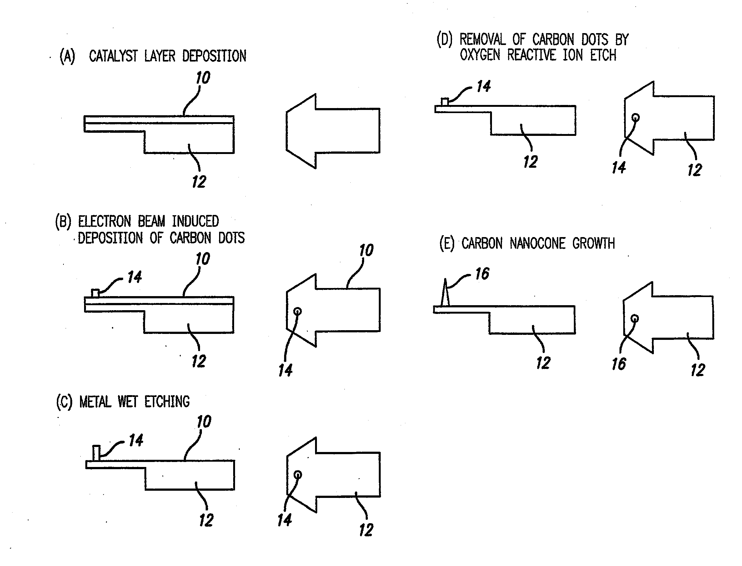
[0053]The present invention relates to a novel method of fabricating a single or an array of high-aspect-ratio nanotips on any type of substrate or cantilever, such as Si, Si-nitri...


PUM

PropertyMeasurementUnit
diameteraaaaaaaaaa
diameteraaaaaaaaaa
pressureaaaaaaaaaa

Abstract

A mechanically stable and oriented scanning probe tip comprising a carbon nanotube having a base with a gradually decreasing diameter, with a sharp tip at the probe tip. Such a tip or an array of tips is produced by depositing a catalyst metal film on a substrate, depositing a carbon dot on the catalyst metal film, etching away the catalyst metal film not masked by the carbon dot, removing the carbon dot from the catalyst metal film to expose the catalyst metal film and growing a carbon nanotube probe tip on the catalyst metal film. The carbon probe tips can be straight, angled, or sharply bent and have various technical applications.

Description

[0001]This application is a divisional of parent application Ser. No. 12 / 088,223, filed Mar. 26, 2008.BACKGROUND OF THE INVENTION[0002]1. Field of Invention[0003]The present invention relates to scanning probe microscopy systems, in particular, atomic force microscopy systems comprising carbon nanotube tips, and methods for fabricating such tips.[0004]2. Discussion of the Related Art[0005]Scanning probe microscopy (SPM) such as atomic force microscopy (AFM) has been an important and powerful technique for resolving nanoscale features, and thus has been utilized for various scientific, engineering, and biological applications. The key component of SPM is the probe tip, as the resolution of SPM imaging is determined by its sharpness, size and shape. See articles by G. Reiss, et al, “Scanning tunneling microscopy on rough surfaces: tip-shape-limited resolution”, J. Appl. Phys. 67, 1156 (1990), and by J. E. Griffith et al, “Scanning probe metrology”, J. Vac. Sci. Technol. A 10, 674 (199...

Claims


Application Information

Patent Timeline
Patent Type & Authority Applications(United States)
IPC IPC(8): G01Q70/16
CPCB82Y10/00B82Y15/00B82Y30/00B82Y35/00H01J9/025G01Q60/56G01Q70/12G11B9/1409G01Q60/38
Inventor JIN, SUNGHOCHEN, LI-HANCHEN, I-CHEN
Owner JIN SUNGHO
Why Eureka
Try Eureka