Method, apparatus and system of parallel IC test

a technology of parallel ic and test method, applied in the field of parallel ic test method, apparatus and system of integrated circuit, can solve the problems of high testing cost, waste of time, serial test process of wafer, etc., and achieve the effect of more accurate testing

Active Publication Date: 2010-09-23
SHANGHAI XINHAO MICROELECTRONICS
View PDF8 Cites 30 Cited by
  • Summary
  • Abstract
  • Description
  • Claims
  • Application Information

AI Technical Summary

Benefits of technology

[0058]The input path for parallel testing can be placed on the wafer containing the dice. The placement of the input paths on the wafer includes but is not limited to within the DUTs, partially in the dice or outside the dice. The wires that are part of input and output paths can be placed in scribe line, within the dice or through the dice. The wires and apparatus in scribe line will be cut during wafer sawing with no effect on the normal function of the dice. The test pads in corner pad or non-connecting pad position has no effect o

Problems solved by technology

However, the wafer test process is still serial, one die at a time due to the limitation of expensive testing channels.
The long testing time results in a high testing cost.
Each time the probe moves from one die to another die it takes 100 ms˜250 ms, this time is wasted because no test is performed during the move.
This further increases the total testing time and the testing cost.
Besides this, the testing can o

Method used


Image

  • Method, apparatus and system of parallel IC test
  • Method, apparatus and system of parallel IC test
  • Method, apparatus and system of parallel IC test

Examples


second embodiment

[0207]FIG. 22(d) is the Testing wafer 2211 is a larger wafer than the wafer under test 2202. The testing cable 2206 can be directly connected to part of the testing wafer 2211 which is extended beyond the wafer under test 2202, so it solves the problem of testing cable 2206 thickness problem in FIG. 22(c). During testing in this embodiment, the power supply and test stimulation are passed to testing wafer 2211 through testing cables. Then the power supply and test stimulation are passed to the corresponding input pad of every die 2202 on the wafer under test 2202 through solder balls 2212. The operation results of the test stimulation can be compared on the wafer under test. It can also be transferred to testing wafer, using comparators on the testing wafer to compare.

third embodiment

[0208]FIG. 22(e) is the In this embodiment, wafer under test 2215 and testing wafer 2211 are of the same size originally, but one side of wafer under test 2215 was cut off while testing wafer 2211 is still a complete wafer. During testing, the power supply and test stimulation are passed to testing wafer 2211 through testing cable, and then the power supply and test stimulation are passed to the corresponding input pad of every die 2202 through solder ball 2212. The operation result of the test stimulation can be compared on the wafer under test, and it can also be transferred to testing wafer, using comparators on the testing wafer to compare. Only one side of wafer under test 2215 is cut off in the embodiment, but in real application, more than one side can be cut off base on the requirement.

fourth embodiment

[0209]FIG. 22(f) is the Testing wafer 2214 is a wafer with TSV. In this embodiment, testing cable 2216 connects the back side of the testing wafer 2214 instead of the front side. The power supply and test stimulation are passed to wafer under test 2202 through TSV hole. To merely illustrate the technical concept, the pressing apparatus 2210 and clamping device 2208 are omitted.

[0210]In the afore embodiments, the solder ball can be placed on the testing wafer to connect the pads on the wafer under test, or be placed on the wafer under test to connect the pads on the testing wafer, or be placed on both wafer under test and testing wafer to connect to each other.

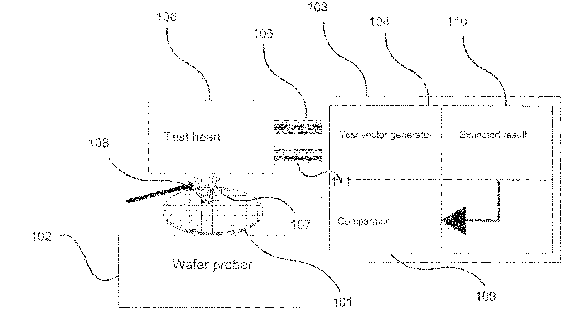
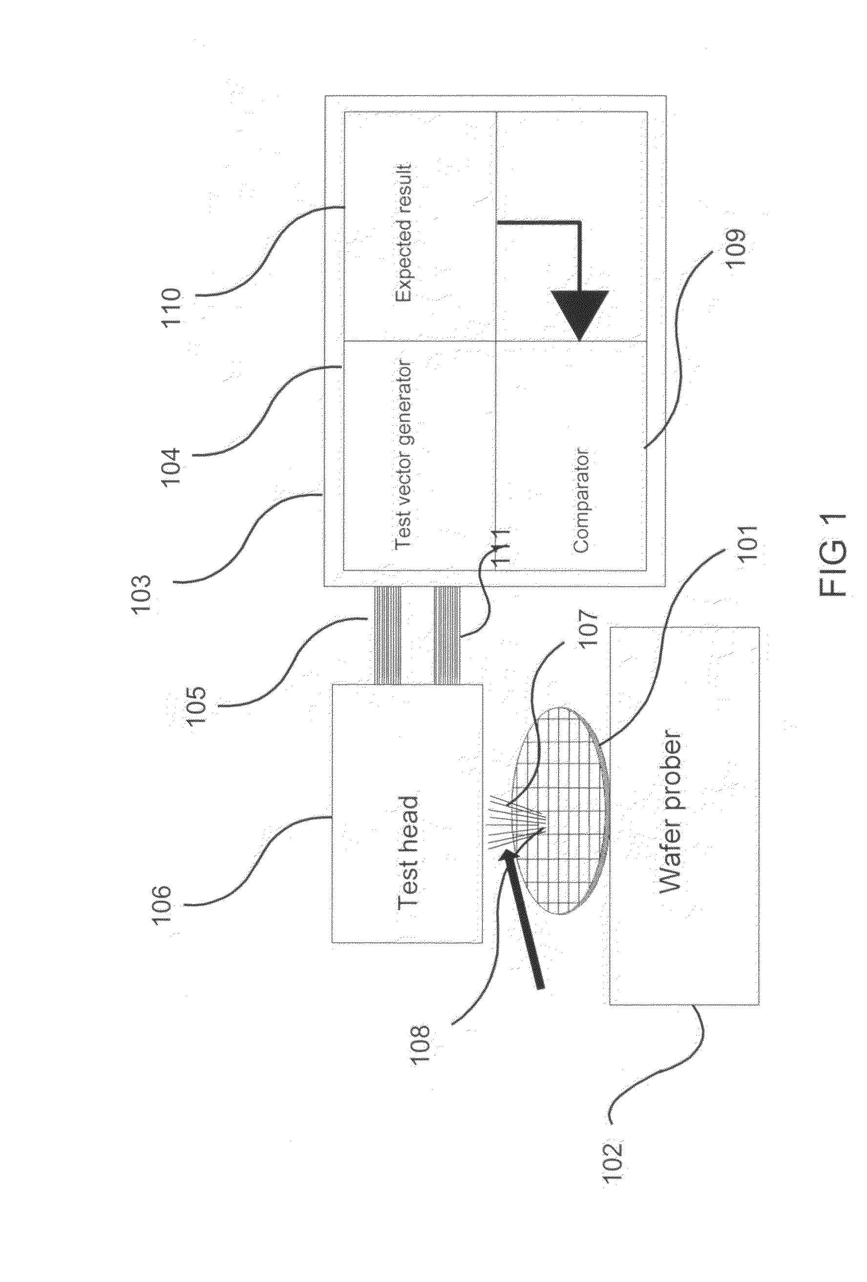
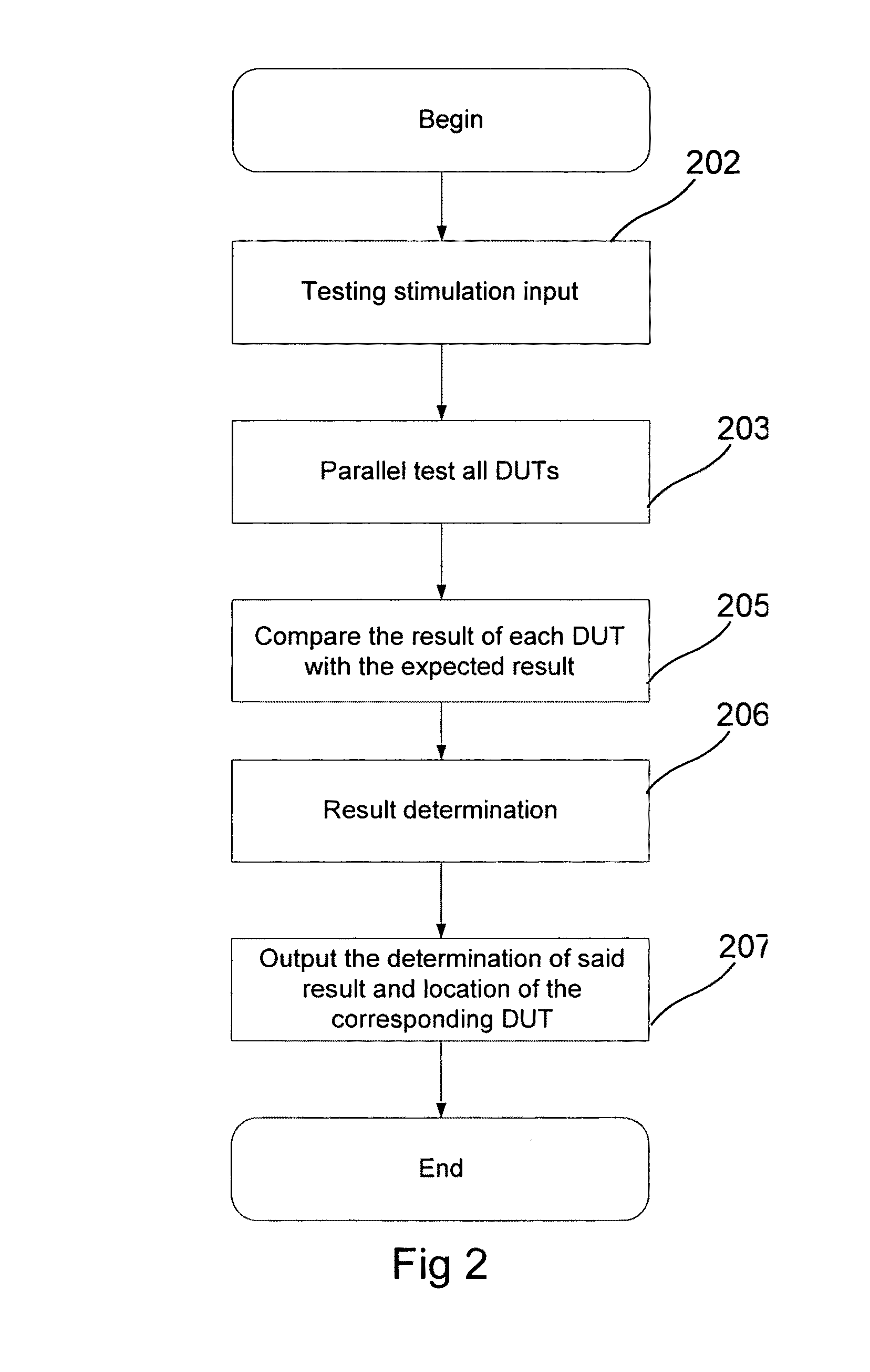
[0211]FIG. 23 illustrates an embodiment of DC characteristic test on a die under test. In this embodiment, a current source 2303 is connected to a pad / solder ball 2302 on a die under test 2301. During the test, the current source 2303 drives a given amount of current to die 2301 through pad / solder ball 2302 to generate a volta...


PUM


Abstract

A method, apparatus and system for integrated circuit testing, wherein a plural number of devices under test (DUTs) and a plural number of comparison apparatuses are placed on a common substrate. The DUTs all operate under the same input stimulation and each produce its own operation output. The outputs are compared by the comparison apparatuses to generate comparison characteristics which are used to filter-out the failed devices. This invention lowers the testing cost, shortens time to product mass-production, and lowers the miss rate of failed devices passed as good ones.

Description

DESCRIPTION OF THE INVENTION[0001]1. Field of the Invention[0002]The present invention is in the area of the integrated circuit, and pertains in particular to a parallel testing method, apparatus and system for integrated circuits.[0003]2. Background of the Invention[0004]In a typical semiconductor manufacturing process a plural number of identical rectangular-shaped integrated circuit dice are fabricated on a thin and uniform wafer of semiconductor material. These said dice on the wafer are separated by scribe lines 60 to 80 microns wide. Often the photo mask alignment mark and wafer acceptance test devices (WAT) are placed in the scribe lines.[0005]During the fabrication process the photo lithography machine exposes one stepper field at a time; each stepper field contains a singular or a plural number of dice. Each said die on the wafer is tested after all manufacture steps are completed. The wafer prober contacts the pads of the dice under test through a probe card, delivering te...

Claims


Application Information

Patent Timeline
IPC IPC(8): G01R31/02
CPCG01R19/16566G01R31/3025G01R31/2851
Inventor LIN, KENNETH CHENGHAOGENG, HONGXIREN, HAOQIZHANG, BINGCHUNZHEN, CHANGCHUN
Owner SHANGHAI XINHAO MICROELECTRONICS
Why Eureka
Try Eureka