

Organic electroluminescent device and method for manufacturing the same
- Summary
- Abstract
- Description
- Claims
- Application Information
AI Technical Summary
Benefits of technology
Problems solved by technology
Method used
Image

Examples
first embodiment
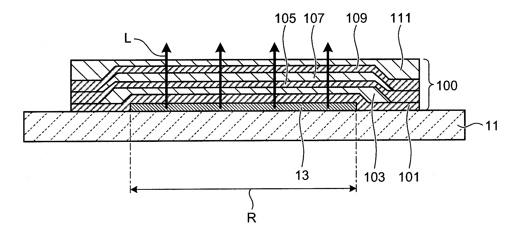
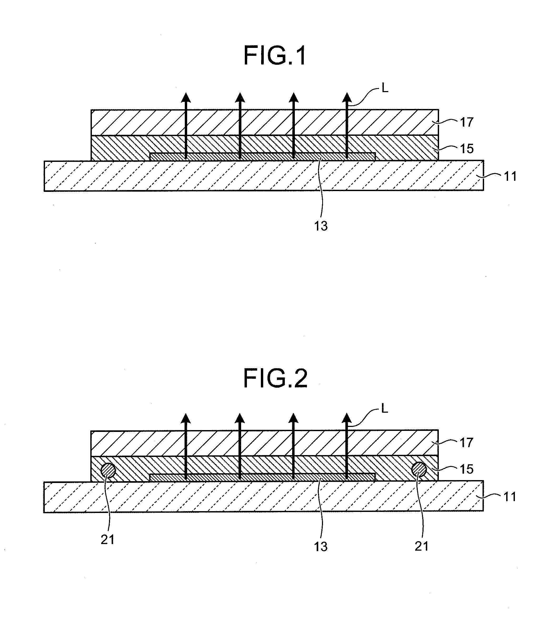
1. First Embodiment
[0049]FIG. 1 is a schematic diagram of a structure of an organic EL device according to the first embodiment of the present invention. The organic EL device according to the present embodiment has a constitution which an organic EL element having an organic layer including at least an organic light-emitting layer is sandwiched between a supporting substrate and a sealing substrate, and the device has a top emission structure such that light L is emitted from a side opposite to the supporting substrate (sealing substrate side). As shown in FIG. 1, the organic EL device according to the present embodiment is composed of a first substrate 11, an organic EL element 13, a binder (resin layer) 15, and a second substrate 17.
[0050]1.1 First Substrate
[0051]The first substrate 11, which is a plate-form substrate, is a supporting substrate having the organic EL element 13 formed on a mounting surface which is one plane surface of the substrate. With respect to the first subs...
second embodiment
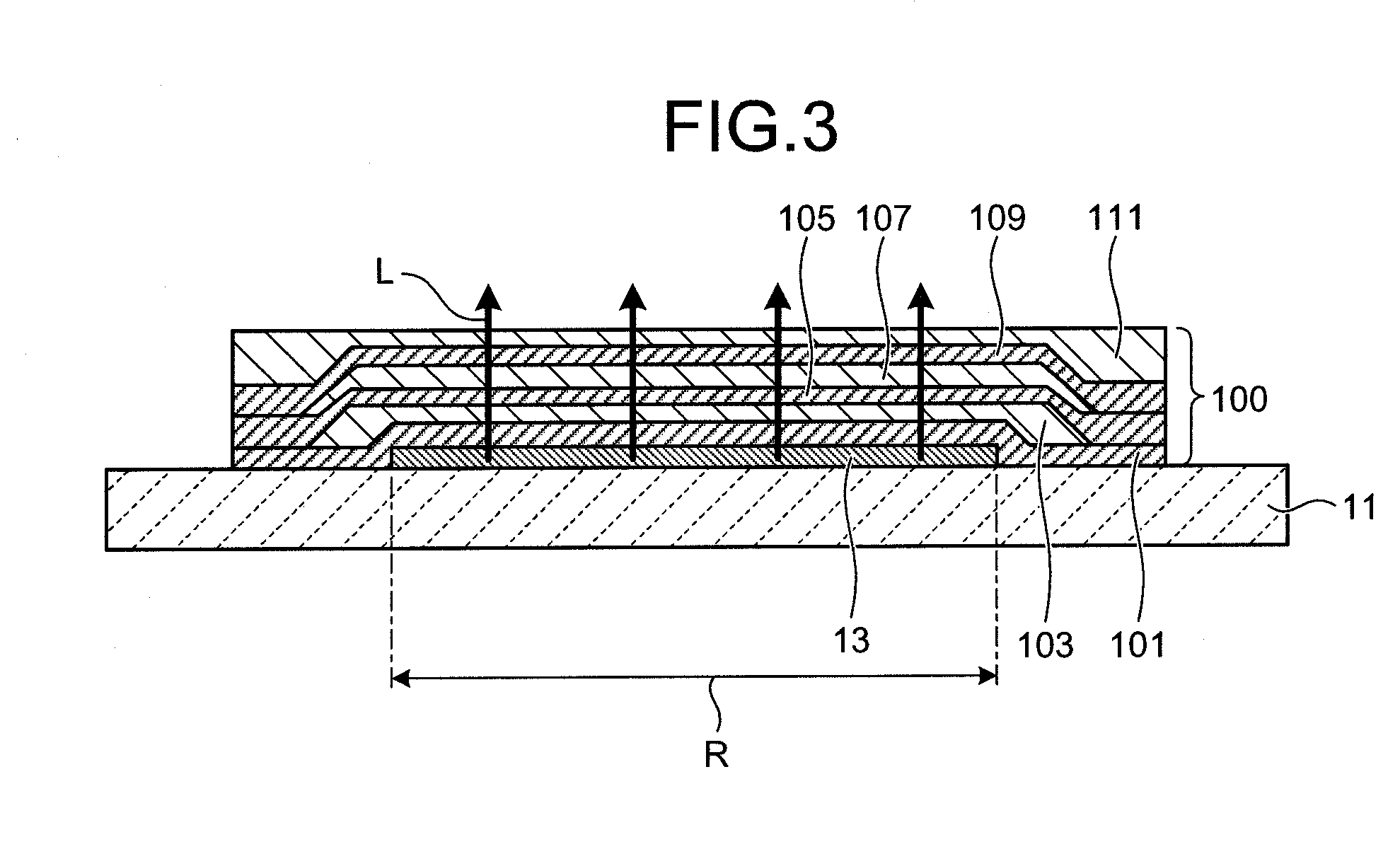
2. Second Embodiment
2.1 Structure of Organic EL Device According to Second Embodiment
[0112]In the second embodiment, an organic EL device having, instead of the second substrate as a sealing substrate, a sealing layer (sealing film) that blocks the organic EL element from ambient air is described.
[0113]FIG. 3 depicts a schematic structure of an organic EL device according to the second embodiment of the present invention. The organic EL device according to the present embodiment is an organic EL device having a structure such that the organic EL device has sandwiched between a supporting substrate and a sealing layer an organic EL element having an organic layer, and having a top emission structure in which light is emitted from the side opposite the supporting substrate (sealing layer side). As shown in FIG. 3, the organic EL device according to the present embodiment is composed of the first substrate 11, the organic EL element 13, and a sealing layer (sealing film) 100.
[0114]A di...
example 1
[0133]In Example 1, the organic EL device having a top emission structure described above in the first embodiment is produced. Chromium (Cr) and indium tin oxide (ITO) are first stacked in this order by a known method on a transparent glass substrate as a first substrate, and patterned to form a first electrode. Then, surface cleaning treatment on the ITO is performed by a UV-ozone treatment apparatus.
[0134]Subsequently, an aqueous solution of PEDOT / PPS (Baytron P (product name), by Bayer AG) as a material for hole injection layer is applied by a spin coating method, and the applied aqueous solution is dried to form a hole injection layer having a thickness of 100 nanometers. A 1% by weight toluene-anisole mixture solution of MEH-PPV (poly(2-methoxy-5-(2′-ethyl-hexyloxy)-paraphenylenevinylene)), by Aldrich Corporation, having a weight average molecular weight of about 200,000 as a luminescent material is prepared. The mixture solution is applied by a spin coating method, and the app...
PUM
 Abstract
Description
Claims
Application Information