Reducing silicide resistance in silicon/germanium-containing drain/source regions of transistors

Active Publication Date: 2010-09-30
GLOBALFOUNDRIES US INC
View PDF10 Cites 31 Cited by
  • Summary
  • Abstract
  • Description
  • Claims
  • Application Information

AI Technical Summary

Benefits of technology

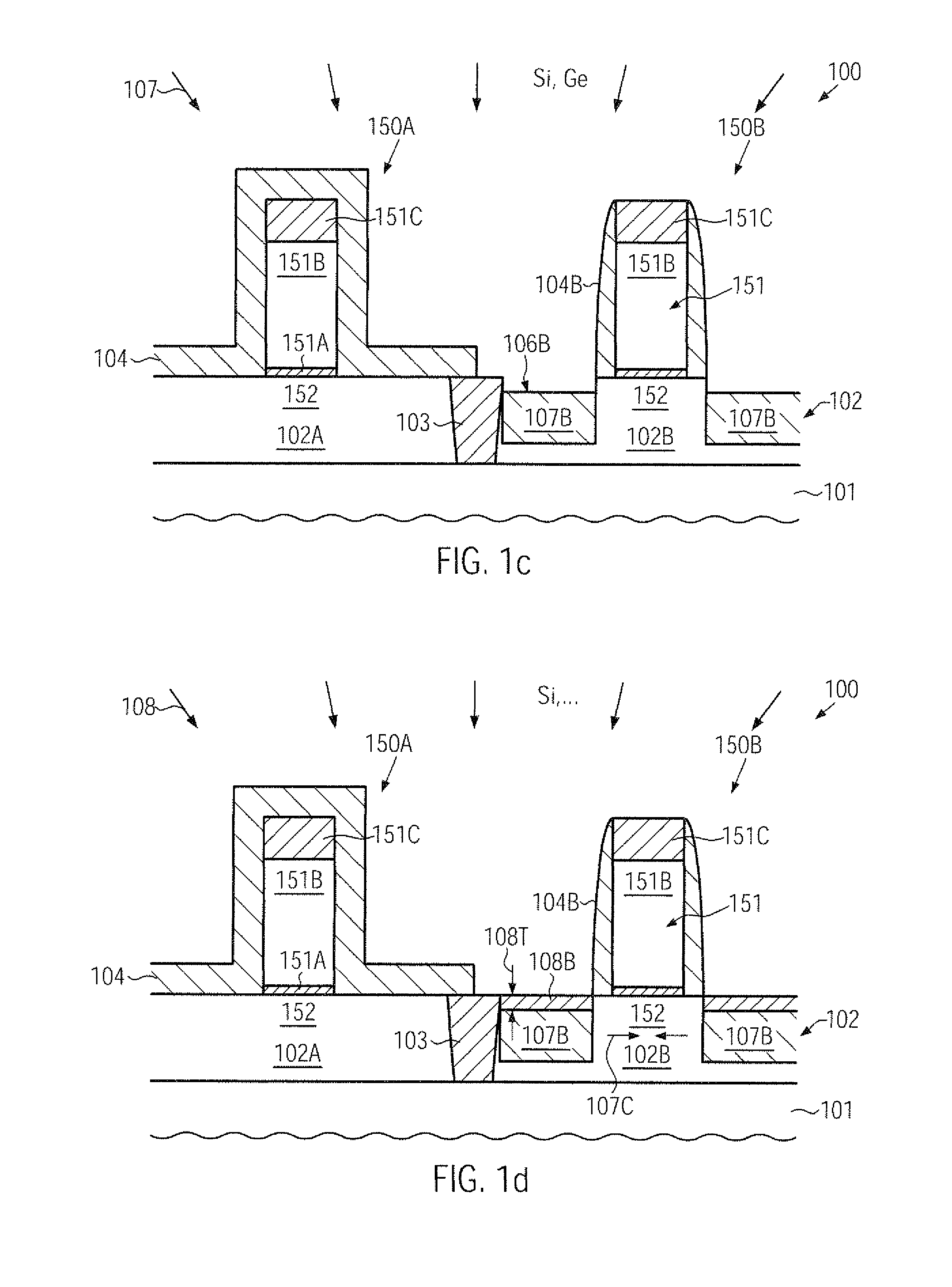
[0013]Generally, the subject matter disclosed herein relates to semiconductor devices and techniques in which a strained silicon/germanium alloy with a moderately high germanium concentration may be used without requiring significant overfill, while also reducing process irregularities during the formation of a metal silicide material. For this purpose, a semiconductor material having a significantly reduced germanium concentration may be formed on the silicon/germanium alloy at an appropriate manufacturing stage so as to provide a silicon-containing semiconductor material for the formation of metal silicide, thereby significantly reducing the probability of creating unstable metal silicide materials, which may frequently be encountered in conventional strategies in which high germanium concentration may be required. The silicon-containing semiconductor material may be provided in the form of a substantially “pure” silicon material, i.e., a silicon material including a dopant species in accordance with a corresponding dopant concentration, while substantially avoiding the incorporation of other atomic species, such as germanium, so as to provide similar process conditions in semiconductor areas having formed therein a silicon/germanium alloy and other semiconductor areas without a strain-inducing silicon/germanium alloy. In other illustrative embodiments disclosed herein, at least a signifi

Problems solved by technology

Moreover, due to the increased covalent radius of the specific atomic species, a moderately low concentration thereof may als

Method used


Image

  • Reducing silicide resistance in silicon/germanium-containing drain/source regions of transistors
  • Reducing silicide resistance in silicon/germanium-containing drain/source regions of transistors
  • Reducing silicide resistance in silicon/germanium-containing drain/source regions of transistors

Examples


Embodiment Construction

[0024]Various illustrative embodiments of the invention are described below. In the interest of clarity, not all features of an actual implementation are described in this specification. It will of course be appreciated that in the development of any such actual embodiment, numerous implementation-specific decisions must be made to achieve the developers' specific goals, such as compliance with system-related and business-related constraints, which will vary from one implementation to another. Moreover, it will be appreciated that such a development effort might be complex and time-consuming, but would nevertheless be a routine undertaking for those of ordinary skill in the art having the benefit of this disclosure.

[0025]The present subject matter will now be described with reference to the attached figures. Various structures, systems and devices are schematically depicted in the drawings for purposes of explanation only and so as to not obscure the present disclosure with details ...


PUM


Abstract

In sophisticated P-channel transistors, a high germanium concentration may be used in a silicon/germanium alloy, wherein an additional semiconductor cap layer may provide enhanced process conditions during the formation of a metal silicide. For example, a silicon layer may be formed on the silicon/germanium alloy, possibly including a further strain-inducing atomic species other than germanium, in order to provide a high strain component while also providing superior conditions during the silicidation process.

Description

BACKGROUND OF THE INVENTION[0001]1. Field of the Invention[0002]Generally, the present disclosure relates to integrated circuits, and, more particularly, to transistors having enhanced performance by using a silicon / germanium (Si / Ge) in the drain / source regions to enhance charge carrier mobility in the channel region of the transistor.[0003]2. Description of the Related Art[0004]The fabrication of integrated circuits requires the formation of a large number of circuit elements, wherein the field effect transistor may represent an important component in advanced logic circuit designs. Generally, a plurality of process technologies are currently practiced for forming field effect transistors, wherein, for complex circuitry, such as microprocessors, storage chips and the like, CMOS technology is currently the most promising approach due to the superior characteristics in view of operating speed and / or power consumption and / or cost efficiency. During the fabrication of complex integrate...

Claims


Application Information

Patent Timeline
IPC IPC(8): H01L29/417H01L21/336H01L29/78
CPCH01L21/02381H01L21/02532H01L21/02535H01L21/0262H01L21/02636H01L29/7848H01L21/823807H01L21/823814H01L29/665H01L29/66636H01L29/7833H01L21/28518
Inventor KRONHOLZ, STEPHANPAPAGEORGIOU, VASSILIOSWIATR, MACIEJ
Owner GLOBALFOUNDRIES US INC
Why Eureka
Try Eureka