Configuration and fabrication of semiconductor structure having bipolar junction transistor in which non-monocrystalline semiconductor spacing portion controls base-link length

a technology of bipolar junction transistor and spacing portion, which is applied in the field of semiconductor technology, can solve the problems of weakened analog performance, many requirements imposed on analog igfet performance conflicting with the results of digital scaling, and poor parameter matching in digital circuitry, and achieves significant reduction of base resistance, enhancing lot-to-lot repeatability of bjt characteristics, and strong control of base-link length lbl

Active Publication Date: 2010-09-30
NAT SEMICON CORP
View PDF4 Cites 20 Cited by
  • Summary
  • Abstract
  • Description
  • Claims
  • Application Information

AI Technical Summary

Benefits of technology

[0050]In short, the present invention furnishes BJTs with well-controlled base-link length LBL. The lot-to-lot repeatability of the BJT characteristics is significantly enhanced. The stronger control of base-link length LBL enables the base resistance to be signi

Problems solved by technology

Although it would be economically attractive to utilize the same transistors for the analog and digital blocks, doing so would typically lead to weakened analog performance.
Many requirements imposed on analog IGFET performance conflict with the results of digital scaling.
Because the resultant dimensional spreads are inherently large, parameter matching in dig

Method used


Image

  • Configuration and fabrication of semiconductor structure having bipolar junction transistor in which non-monocrystalline semiconductor spacing portion controls base-link length
  • Configuration and fabrication of semiconductor structure having bipolar junction transistor in which non-monocrystalline semiconductor spacing portion controls base-link length
  • Configuration and fabrication of semiconductor structure having bipolar junction transistor in which non-monocrystalline semiconductor spacing portion controls base-link length

Examples


Embodiment Construction

List of Contents

[0070]A. Reference Notation and Other Preliminary Information

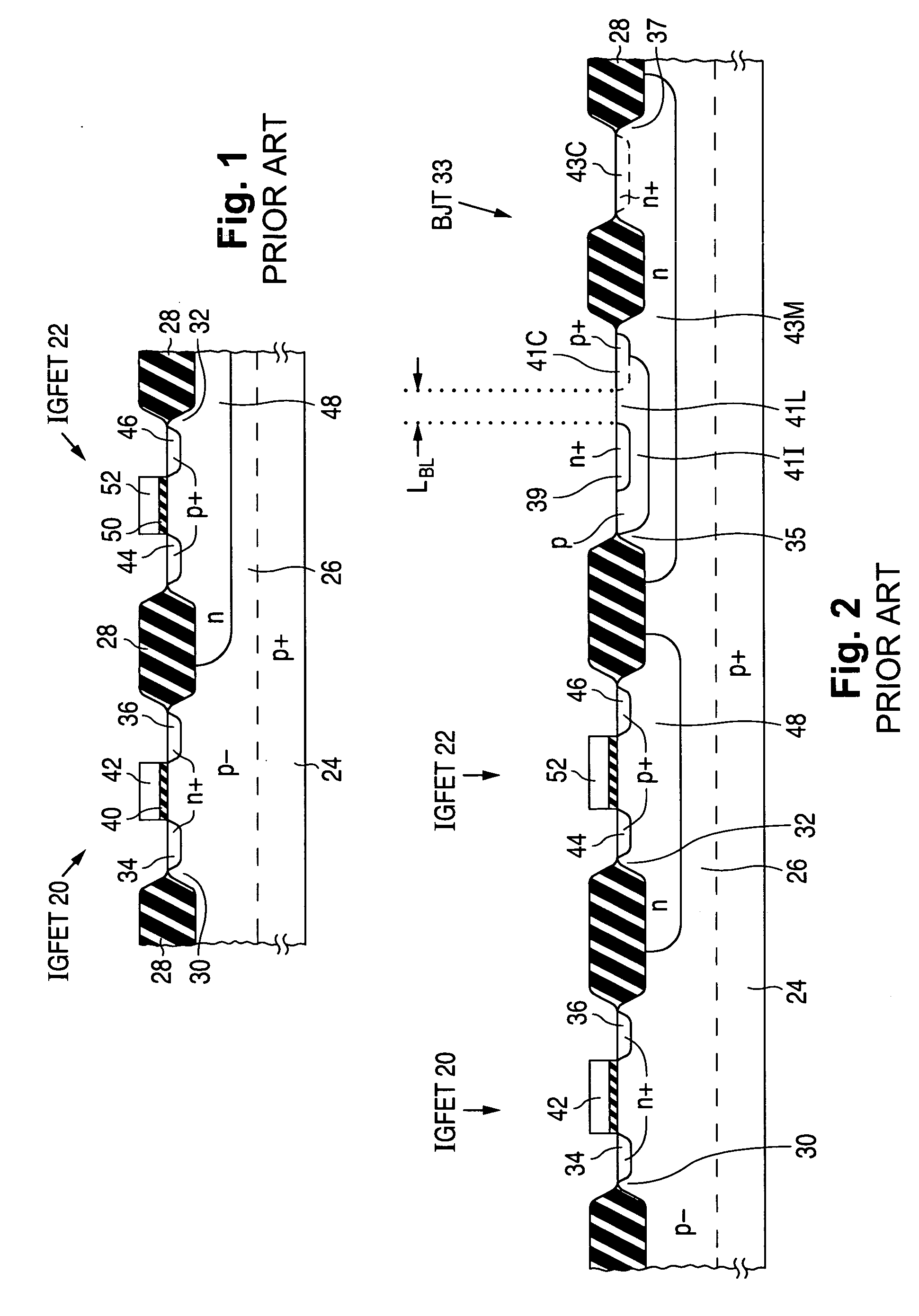
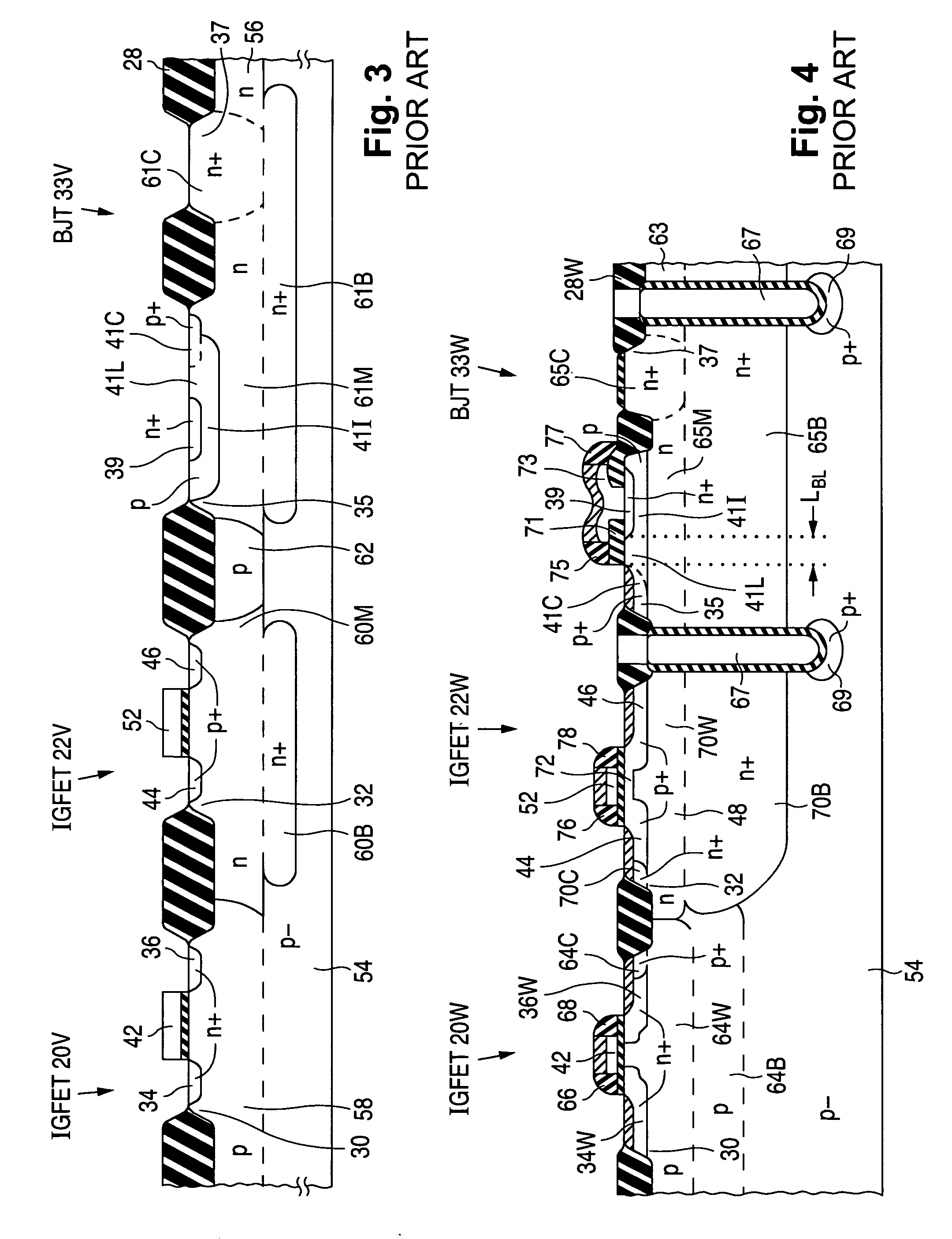
[0071]B. Complementary-BJT / Complementary-IGFET Structures Suitable for Mixed-signal Applications

[0072]C. Well Architecture and Doping Characteristics

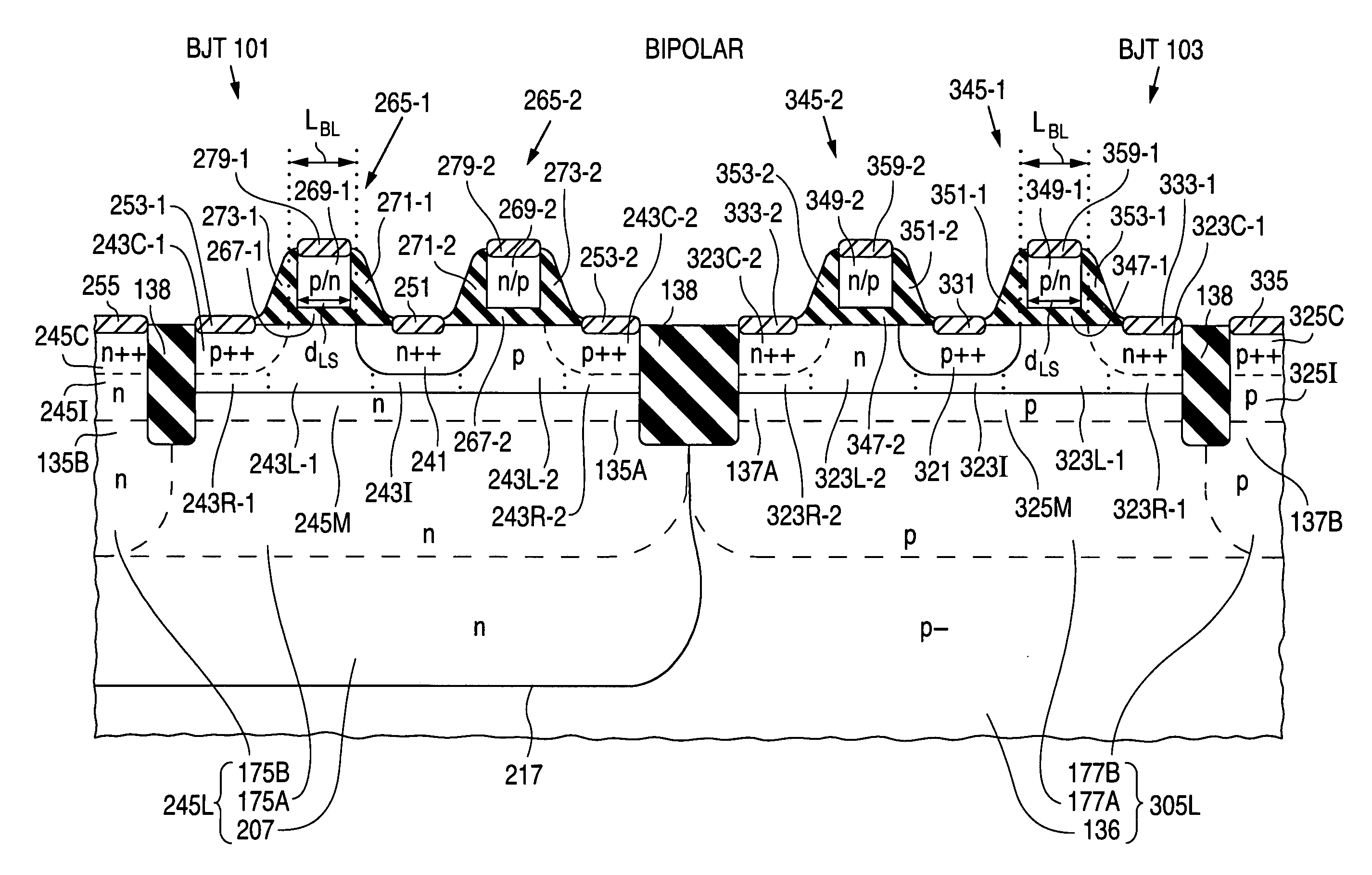
[0073]D. Bipolar Junction Transistors[0074]D1. Structure of Npn Transistor[0075]D2. Control of Base-link Length in Npn Transistor[0076]D3. Pnp Transistor[0077]D4. BJT Variations

[0078]E. Asymmetric High-voltage IGFETs[0079]E1. Structure of Asymmetric High-voltage N-channel IGFET[0080]E2. Source / Drain Extensions of Asymmetric High-voltage N-channel IGFET[0081]E3. Structure of Asymmetric High-voltage P-channel IGFET[0082]E4. Source / Drain Extensions of Asymmetric High-voltage P-channel IGFET

[0083]F. Extended-drain IGFETs[0084]F1. Structure of Extended-drain N-channel IGFET[0085]F2. Operational Physics of Extended-drain N-channel IGFET[0086]F3. Structure of Extended-drain P-channel IGFET[0087]F4. Operational Physics of Extended-drain P-channel IGFET

[0088]G. Symmetri...


PUM


Abstract

A semiconductor structure contains a bipolar transistor (101) and a spacing structure (265-1 or 265-2). The transistor has an emitter (241), a base (243), and a collector (245). The base is formed with an intrinsic base portion (243I), a base link portion (243L), and a base contact portion (245C). The intrinsic base portion is situated below the emitter and above material of the collector. The base link portion extends between the intrinsic base portion and the base contact portions. The spacing structure includes an isolating dielectric layer (267-1 or 267-2) and a spacing component. The dielectric layer extends along the upper semiconductor surface. The spacing component includes a lateral spacing portion (269-1 or 269-2) of largely non-monocrystalline semiconductor material, preferably polycrystalline semiconductor material, situated on the dielectric layer above the base link portion. Opposite first and second upper edges of the lateral spacing portion (275-1 and 277-1) laterally conform to opposite first and second lower edges (297-1 and 299-1) of the base link portion so as to determine, and thereby control, its length.

Description

CROSS-REFERENCE TO RELATED APPLICATIONS[0001]This application is related to the following U.S. patent applications all filed on the same date as this application: U.S. patent application Ser. No. ______ (Bulucea et al.), attorney docket no. NS-7005 US, U.S. patent application Ser. No. ______ (Bulucea et al.), attorney docket no. NS-7040 US, U.S. patent application Ser. No. ______ (Parker et al.), attorney docket no. NS-7192 US, U.S. patent application Ser. No. ______ (Bahl et al.), attorney docket no. NS-7210 US, U.S. patent application Ser. No. ______ (Yang et al.), attorney docket no. NS-7313 US, and U.S. patent application Ser. No. ______ (Bulucea et al.), attorney docket no. NS-7433 US, U.S. patent application Ser. No. ______ (Bulucea et al.), attorney docket no. NS-7434 US, U.S. patent application Ser. No. ______ (French et al.), attorney docket no. NS-7435 US, U.S. patent application Ser. No. ______ (Bulucea et al.), attorney docket no. NS-7436 US, and U.S. patent application ...

Claims


Application Information

Patent Timeline
IPC IPC(8): H01L27/06H01L27/082H01L21/8228H01L21/8249
CPCH01L21/82285H01L27/0826H01L27/0623H01L21/8249
Inventor YANG, JENG-JIUNBULUCEA, CONSTANTIN
Owner NAT SEMICON CORP
Why Eureka
Try Eureka