Light-emitting display and method of manufacturing the same

a technology of light-emitting display and top-emitting system, which is applied in the manufacture of electrode systems, electric discharge tubes/lamps, and discharge tubes luminescnet screens, etc., can solve the problems of large voltage drop in this part, easy oxidation of the surface of auxiliary wiring, and increased power consumption of displays, so as to prevent the increase of connection resistance and improve the effect of display quality and low power consumption

Active Publication Date: 2010-09-30
JOLED INC
View PDF11 Cites 47 Cited by
  • Summary
  • Abstract
  • Description
  • Claims
  • Application Information

AI Technical Summary

Benefits of technology

[0015]According to the light-emitting display or the method of manufacturing a light-emitting display of the invention, the second electrode and the auxiliary wiring are electrically connected to each other through the conductive contact section, so even

Problems solved by technology

However, in the above-described technique in Patent Document 1, in the case where, for example, aluminum (Al) or an Al alloy is used for a surface of an electrode on a drive panel side, when the auxiliary wiring is formed of the same material as that of the electrode, the surface of the auxiliary wiring is easily oxidized.
When the surface is oxidized, connection resistance between the auxiliary wiring and the electrode on the light

Method used


Image

  • Light-emitting display and method of manufacturing the same
  • Light-emitting display and method of manufacturing the same
  • Light-emitting display and method of manufacturing the same

Examples


first embodiment

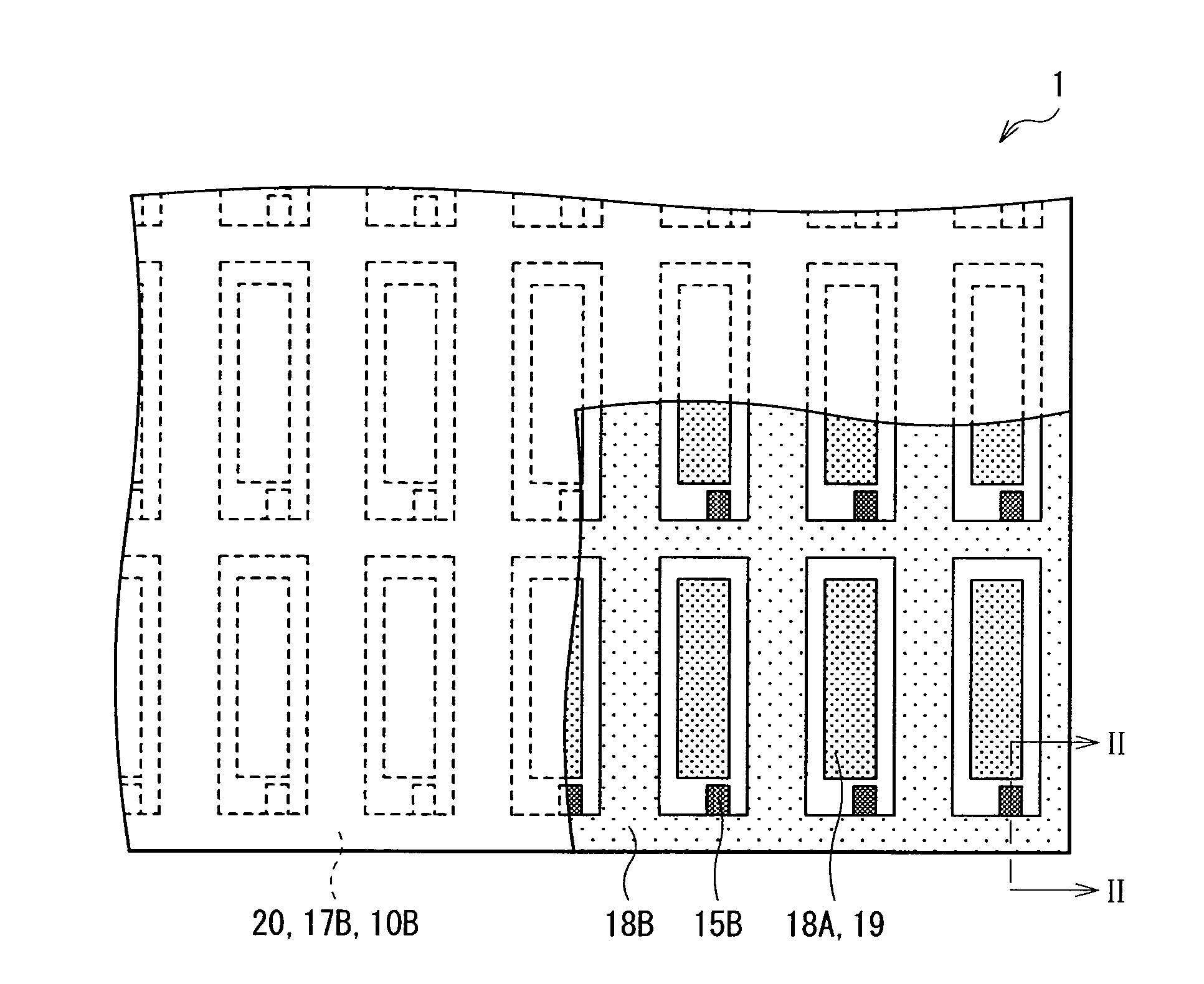
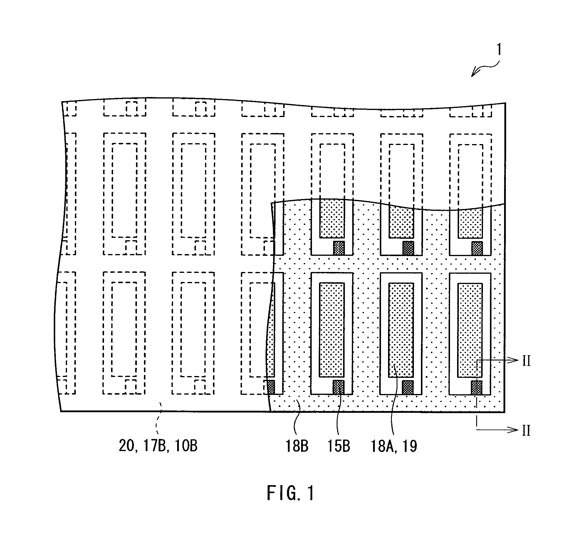
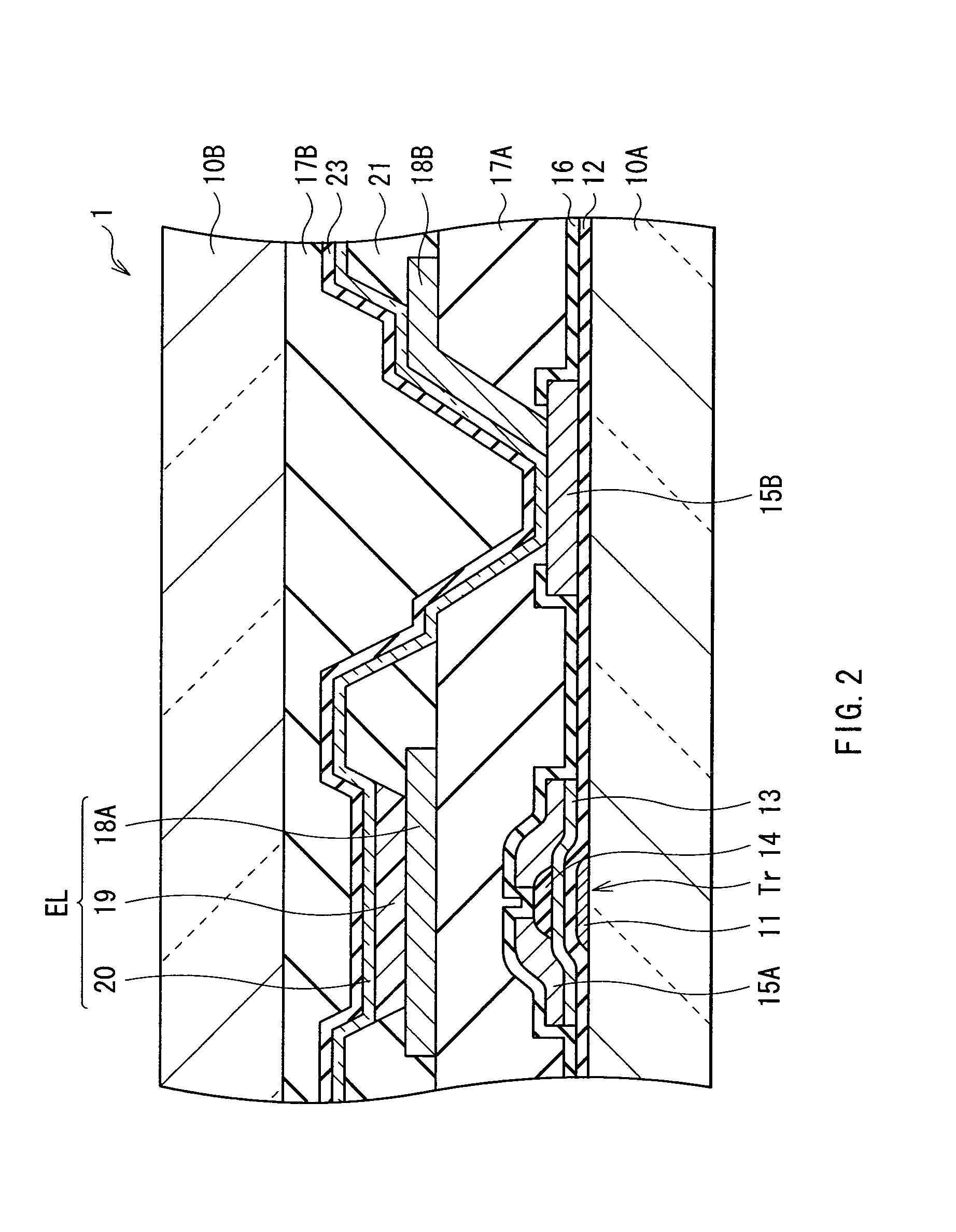
[0038]FIGS. 1 and 2 show the configuration of a light-emitting display (an organic EL display 1) according to a first embodiment of the invention, and

[0039]FIG. 1 shows a plan configuration and FIG. 2 shows a sectional configuration taken along a line II-II of FIG. 1.

[0040]The organic EL display 1 has a laminate configuration in which a multilayer film is laminated between a pair of insulating transparent substrates 10A and 10B. More specifically, a gate electrode 11, a gate insulating film 12, a silicon film 13, a stopper insulating film 14 and a wiring layer 15A are laminated from the transparent substrate 10A side to constitute a thin film transistor Tr. Moreover, a passivation insulating film 16 and a planarization insulating film 17A are laminated on the thin film transistor Tr. On the planarization insulating film 17A, an organic EL element EL is formed corresponding to a region where the thin film transistor Tr is formed.

[0041]Each organic EL element EL has a laminate configu...

second embodiment

[0077]Next, a light-emitting display according to a second embodiment of the invention will be described below. In addition, like components are denoted by like numerals as of the first embodiment and will not be further described.

[0078]FIG. 9 shows a sectional configuration of the light-emitting display (an organic EL display 2) according to the embodiment. In the organic EL display 2, a contact section 22A is formed in the same layer as the first electrode 18A and an auxiliary wiring 18C instead of the same layer as the wiring layer 15A. However, the contact section 22A is made of a different material from the materials of the first electrode 18A and the auxiliary wiring 18C. More specifically, as the contact section 22A, such a material that its selectivity is increased at the time of etching the first electrode 18A and the auxiliary wiring 18C is used. Then, as in the case of the first embodiment, the second electrode 20 and the auxiliary wiring 18C are connected to each other t...

third embodiment

[0088]Next, a light-emitting display according to a third embodiment of the invention will be described below. In addition, like components are denoted by like numerals as of the first and second embodiments and will not be further described.

[0089]FIG. 14 shows a sectional configuration of the light-emitting display (an organic EL display 3) according to the embodiment. In the organic EL display 3, the wiring layer 15A and the contact section 15B are a multilayer film in which layers 15A1, 15A2 and 15A3 are laminated in order from the transparent substrate 10A side and a multilayer film in which layers 15B1, 15B2 and 15B3 are laminated in order from the transparent substrate 10A side, respectively. At least an uppermost layer (for example, the layer 15A3 or 15A2 or the layer 15B3 or 15B2) of each of the multilayer films is made of such a material (for example, Mo or Al) that its selectivity is reduced at the time of etching the first electrode 18A and the auxiliary wiring 18B (low e...


PUM


Abstract

A light-emitting display capable of maintaining low power consumption and improving display quality irrespective of the configuration of an auxiliary wiring is provided. A second electrode 20 and an auxiliary wiring 18B are electrically connected to each other through a conductive contact section 15B. Moreover, only a part of the auxiliary wiring 18B is connected to the contact section 15B. Even if the surface of the auxiliary wiring 18B is oxidized, an increase in connection resistance is prevented. Moreover, a restriction on layout is not imposed at the time of forming the contact section 15B.

Description

TECHNICAL FIELD[0001]The present invention relates to a top emission system light-emitting display and a method of manufacturing such a light-emitting display.BACKGROUND ART[0002]In recent years, as one of flat panel displays, organic EL displays displaying an image through the use of an organic EL (Electro Luminescence) phenomenon have received attention. The organic EL displays use the light-emitting phenomenon of an organic light-emitting device, so the organic EL displays have superior characteristics such as a wide viewing angle and low power consumption. Moreover, the organic EL displays have high responsivity to a high-definition high-speed video signal, so the organic EL displays has been developed toward practical use specifically in a video field or the like.[0003]As a drive system in the organic EL displays, an active matrix system using a thin film transistor (TFT) as a drive element is superior in responsivity and resolution, compared to a passive matrix system, and in ...

Claims


Application Information

Patent Timeline
IPC IPC(8): H05B33/06H05B33/10H05B44/00
CPCH01L27/3244H05B33/10H01L51/5228H01L51/5212H10K59/122H10K50/814H10K50/824H01L21/31051H10K59/12
Inventor FUJIOKA, HIROFUMIOZAWA, NOBUO
Owner JOLED INC
Why Eureka
Try Eureka