Mounting structure, electro-optical device, electronic apparatus, and method of producing the mounting structure

a technology of mounting structure and mounting plate, which is applied in the direction of dielectric characteristics, instruments, and the details of semiconductor/solid-state devices, can solve the problems of reducing electrical reliability, cracking, and resinous protruding members, and achieves high electrical reliability and increase the effect of connection resistan

Active Publication Date: 2008-05-01
EPSON IMAGING DEVICES CORP
View PDF5 Cites 0 Cited by
  • Summary
  • Abstract
  • Description
  • Claims
  • Application Information

AI Technical Summary

Benefits of technology

[0009]An advantage of some aspects of the invention is to provide a mounting structure, an electro-optical device, and an electronic apparatus, which have high electrical reliability as a result of restricting variations and an increase in connection resistance by reducing the possibility of a protruding electrode becoming cracked.

Problems solved by technology

When a deformation amount of the protruding electrode is too large, for example, a crack occurs in the aforementioned resinous protruding member or the electrically conductive layer, formed on the protruding member.
This results in variations in electrical conductivity of the protruding electrode and an increase in a resistance value, thereby reducing electrical reliability.
Therefore, it is not possible to eliminate the possibility of, for example, the protruding electrode becoming cracked (as well as deformation of the electrically conductive layer resulting from variations and an increase in resistance.
However, when this is done, contact pressure or contact area may no longer be ensured due to an insufficient deformation amount of the protruding electrode.
Therefore, in either case, variations or an increase in a conductive connection resistance occurs, thereby resulting in improper mounting in extreme cases.
Therefore, the pushing force can be opposed by the second area, so that unnecessary deformation of the protruding electrode during mounting is restricted.
Therefore, for example, cracking of the protruding electrodes occurs rarely.
In particular, when the semiconductor device is mounted to a panel using a hard substrate, such as a glass substrate, deformation of a connecting pad, formed on the hard substrate, cannot be expected.

Method used


Image

  • Mounting structure, electro-optical device, electronic apparatus, and method of producing the mounting structure
  • Mounting structure, electro-optical device, electronic apparatus, and method of producing the mounting structure
  • Mounting structure, electro-optical device, electronic apparatus, and method of producing the mounting structure

Examples


Embodiment Construction

Structure of Electronic Component (Semiconductor Device)

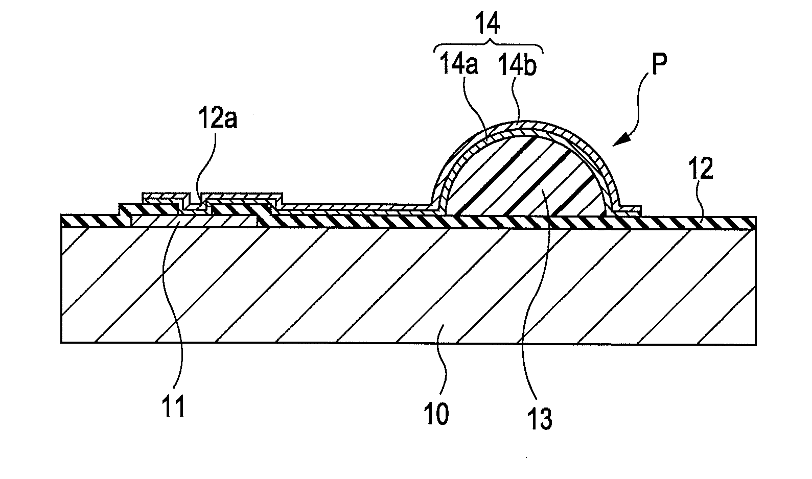
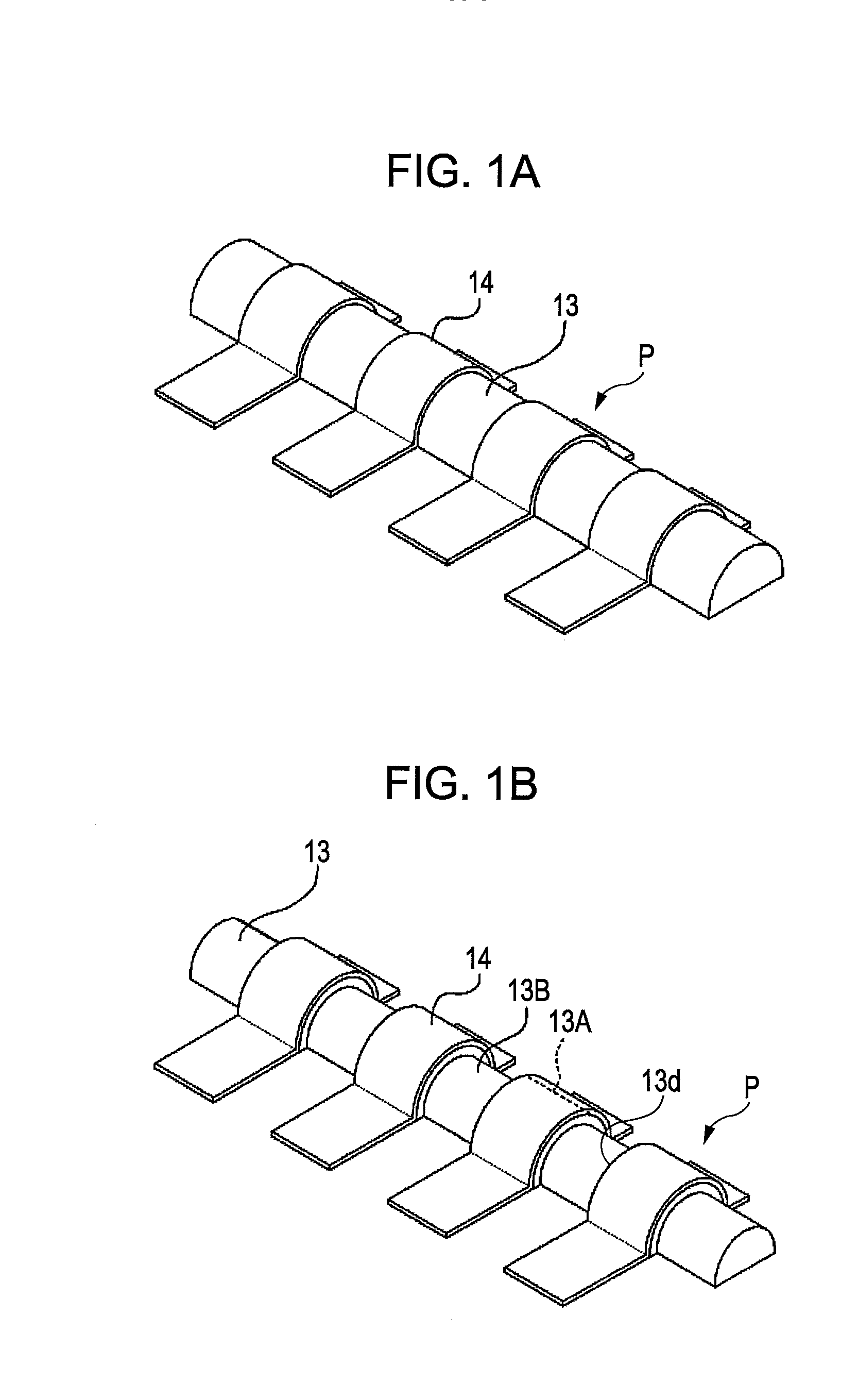
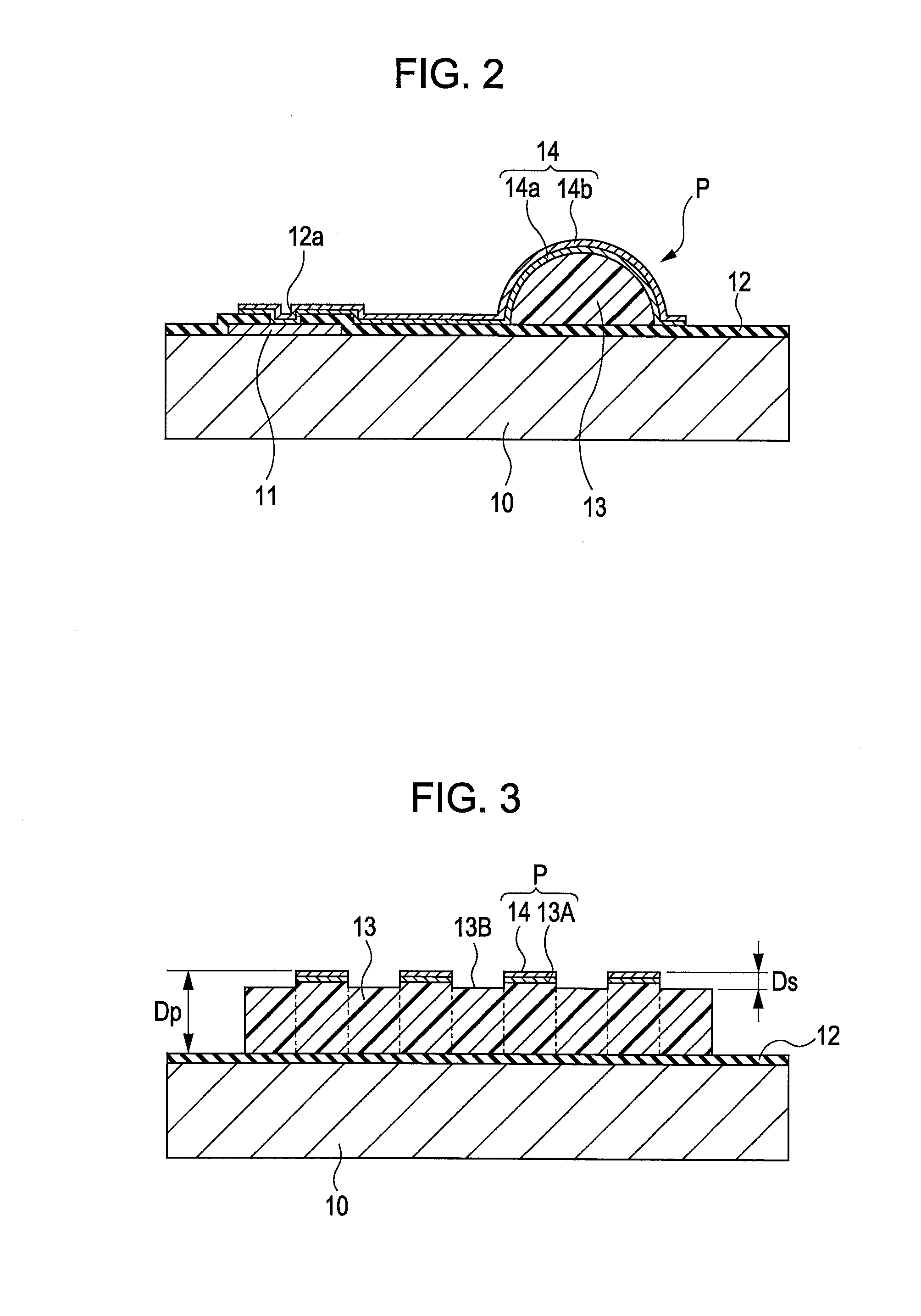
[0037]Next, embodiments of the invention will be described in detail with reference to the attached drawings. FIGS. 1A and 1B are schematic perspective views of protruding electrodes provided at an electronic component, or a semiconductor device, according to an embodiment. FIG. 2 is a partial vertical sectional view of the protruding electrode. FIG. 3 is a vertical sectional view taken along a direction of extension of a protruding member where the protruding electrodes are provided.

[0038]According to the embodiment, as shown in FIG. 2, base electrodes 11 and an insulating layer 12 are formed on a surface of a substrate 10, such as a semiconductor substrate, formed of, for example, a single crystal silicon. The base electrodes 11 are formed of, for example, aluminum. The insulating layer 12 has an opening 12a where a portion of each base electrode 11 is exposed, and is formed of, for example, silicon oxide or silicon nitride. ...


PUM

PropertyMeasurementUnit
thicknessaaaaaaaaaa
thicknessaaaaaaaaaa
thicknessaaaaaaaaaa

Abstract

A mounting structure includes a first electronic component, a second electronic component, and an adhesive. The first electronic component includes at least one protruding electrode including a protruding member and at least one electrically conductive layer. The protruding member is formed of resin. The at least one electrically conductive layer is disposed on the protruding member. The second electronic component has a facing electrode electrically conductively in contact with the at least one protruding electrode. The adhesive is used to adhere the first electronic component and the second electronic component to each other. The protruding member has a first area and a second area. The first area has the at least one electrically conductive layer provided thereon. The second area does not have the at least one electrically conductive layer provided thereon. The first area of the protruding member is squashed more than the second area.

Description

[0001]The entire disclosure of Japanese Patent Application Nos. 2006-292173, filed Oct. 27, 2006 and 2007-146544, filed Jun. 1, 2007 are expressly incorporated by reference herein.BACKGROUND[0002]1. Technical Field[0003]The present invention relates to a mounting structure, an electro-optical device, an electronic apparatus, and a method of producing the mounting structure. More particularly, the invention relates to a structure of a protruding electrode provided at an electronic component.[0004]2. Related Art[0005]In general, various electronic components, such as semiconductor devices, including a protruding electrode (bump electrode), provided on a surface of a substrate so as to protrude therefrom, are known. The protruding electrode is adhered to, for example, a substrate, at a side where mounting is performed, for electrical conduction. In general, a metallic bump electrode, formed by, for example, thickly plating a seed electrode with a metal (such as Au), is used as the prot...

Claims


Application Information

Patent Timeline
Patent Type & Authority Applications(United States)
IPC IPC(8): H01R12/04H01R43/00H05K1/16
CPCG02F1/13452H05K1/111H05K3/305H05K3/326H05K3/4007Y10T29/49169H05K2201/0367H05K2201/09436H05K2201/09909H05K2201/10977H05K2201/0133H01L24/02H01L2224/0235H01L2224/02375H01L2224/05001H01L2224/05022H01L2224/05124H01L2224/05147H01L2224/05155H01L2224/05164H01L2224/05166H01L2224/05171H01L2224/05184H01L2224/05548H01L2224/05639H01L2224/05644H01L2224/05647H01L2224/05669H01L2224/11H01L2224/13008H01L2924/00014H01L2924/01074H01L2924/01023H01L2924/013
Inventor SAITO, ATSUSHI
Owner EPSON IMAGING DEVICES CORP
Why Eureka
Try Eureka