Organic Luminescence Transistor Device and Manufacturing Method Thereof

a luminescence transistor and organ technology, applied in the direction of thermoelectric devices, show cards, instruments, etc., can solve the problem of difficult control of the luminescence amount, and achieve the effect of efficient manufacturing

Inactive Publication Date: 2010-09-30
DAI NIPPON PRINTING CO LTD +2
View PDF2 Cites 24 Cited by
  • Summary
  • Abstract
  • Description
  • Claims
  • Application Information

AI Technical Summary

Benefits of technology

[0010]The present invention is accomplished in order to solve the aforementioned problems. An object of the present invention is to provide a vertical type of organic luminescence transistor device and a manufacturing method thereof wherein a current control between an anode and a cathode is facilitated.
[0030]Preferably, the step of providing the organic EL layer includes the steps of: providing an electric-charge injection layer by applying a coat-type electric-charge injection material onto the first electrode layer at an area not provided with the insulation layer or the layered structure; and providing a luminescent layer on a side of an upper surface of the electric-charge injection layer or on a side of an upper surface of the electric-charge-injection inhibiting layer and the electric-charge injection layer; wherein the organic EL layer is formed by the electric-charge injection layer and the luminescent layer; and the step of providing the second electrode layer includes a step of providing the second electrode layer on a side of an upper surface of the luminescent layer. In this case, since the electric-charge injection layer is provided by applying the coat-type electric-charge injection material, the electric-charge injection material can very easily reach the edge portion of the assistance electrode located inside the edge portion of the electric-charge-injection inhibiting layer.

Problems solved by technology

Thus, the amount of the generated electric charges cannot be controlled by controlling the voltage (Vg) to be applied between the assistance electrode 113 and the anode 115, so that it is difficult to control the amount of the luminescence.

Method used


Image

  • Organic Luminescence Transistor Device and Manufacturing Method Thereof
  • Organic Luminescence Transistor Device and Manufacturing Method Thereof
  • Organic Luminescence Transistor Device and Manufacturing Method Thereof

Examples


example 1

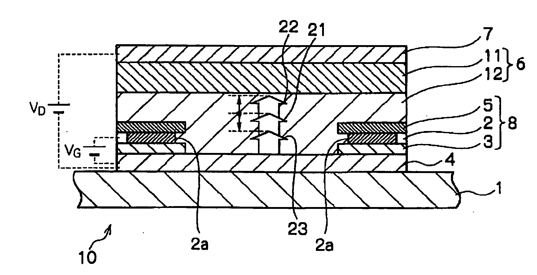
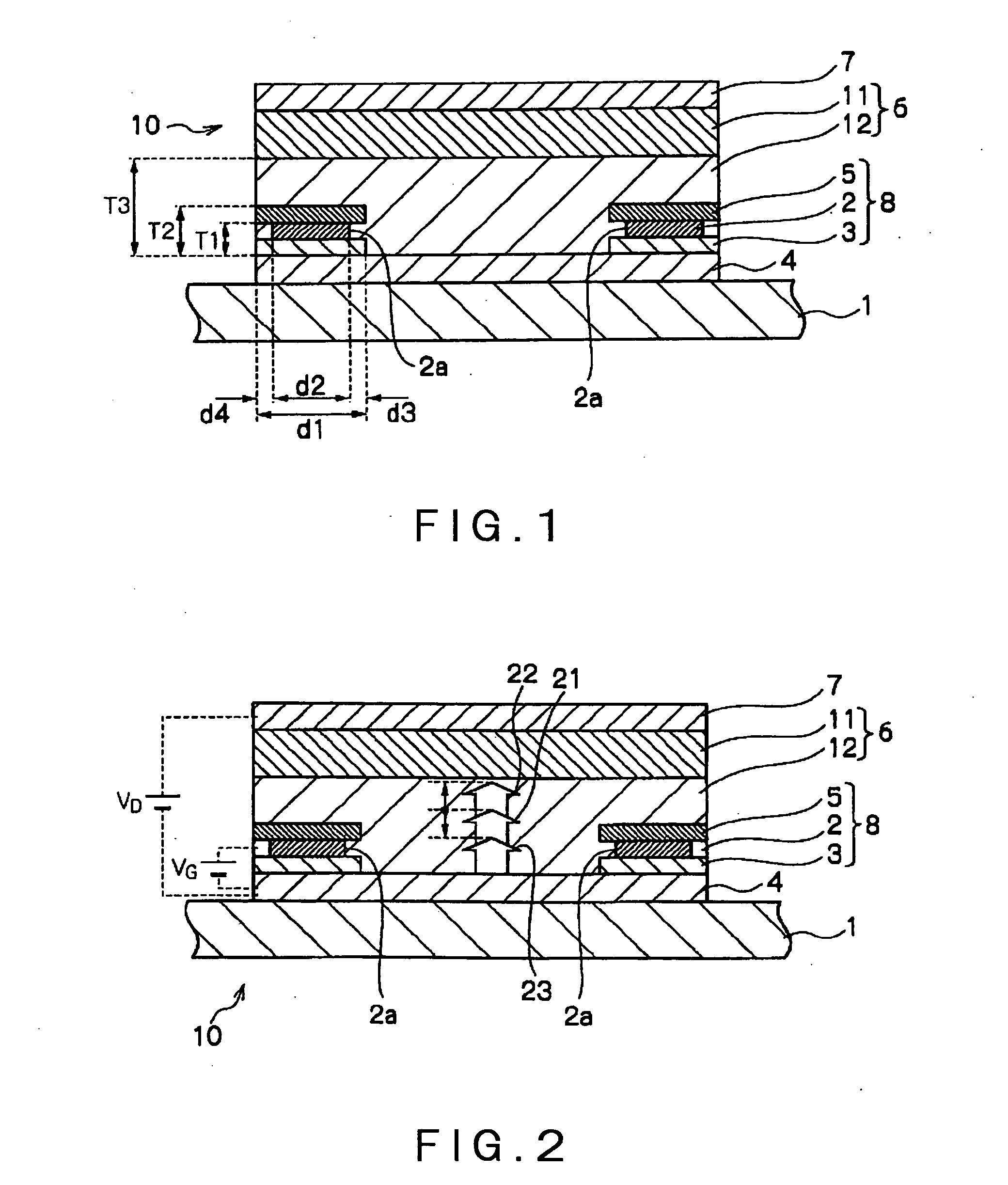
[0155]A laminar insulation layer 3′ was formed into a 100 nm thickness, by means of a sputtering of SiO2, on a glass substrate 1 having a first electrode 4 (anode) that is made of an ITO film and has a 100 nm thickness. Then, on the laminar insulation layer 3′, a resist for an etching process (manufactured by TOKYO OHKA KOGYO CO. Ltd., trade name: OFPR800) was applied into a 2 μm thickness, exposed and developed, so that a resist pattern of a comb-like shape having a wideness d1 of 100 μm was formed. By using the resist pattern as a mask, the laminar insulation layer 3′ was dry-etched and thus patterned, so that an insulation layer 3 having the comb-like shape of the thickness of 100 nm and the wideness d1 of 100 μm was formed. Thereafter, the resist for an etching process was peeled off by a peeling solution (manufactured by TOKYO OHKA KOGYO CO. Ltd., trade name: Peeling Solution 104). Next, a laminar assistance electrode 2 was formed into a 30 nm thickness, by means of a sputterin...

example 2

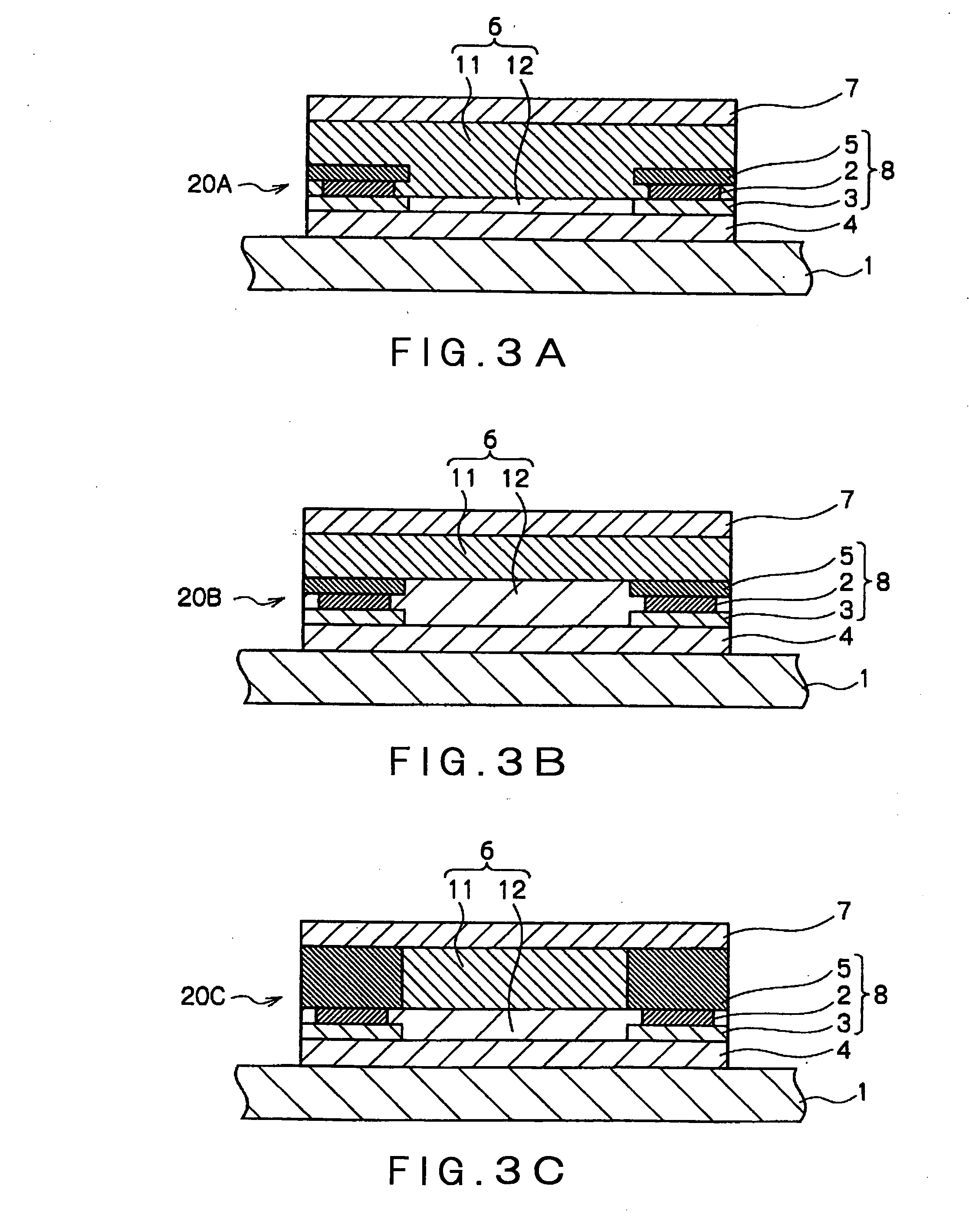
[0159]A polyfluorene (manufactured by AMERICAN DYE SOURCE Inc., trade name: Poly[(9,9-dioctylfluorenyl-2,7-diyl)-co-(N,N′-diphenyl)-N,N′-di(p-butylphenyl)1,4-diamino-benzene)])]) as an electric-charge injecting material was applied by means of an ink-jetting method, so that an electric-charge injection layer 12 was formed into a thickness of 200 nm, which was smaller than the thickness of the layered structure 8 (consisting of the insulation layer 3, the assistance electrode 2 and the electric-charge injection inhibiting layer 5). Except the above, in the same manner as the example 1, an organic luminescent transistor device of the example 2 as shown in FIG. 19 was manufactured.

example 3

[0160]Before the laminar insulation layer 3′ was formed on the first electrode 4, as an electric-charge (positive-hole) injection layer 12, a poly(3,4)ethylene-dioxy-thiophene / polystyrene-sulphonate (PEDOT / PSS, manufactured by BAYER AG, trade name: Baytron P CH8000) was deposited into a 80 nm thickness by means of a spin coating method, on the first electrode 4. Except the above, in the same manner as the example 1, an organic luminescent transistor device of the example 3 as shown in FIG. 20 was manufactured.


PUM


Abstract

Disclosed is an organic light-emitting transistor device comprising a substrate, a first electrode layer formed on the upper side of the substrate, a multilayer structure formed locally on the upper side of the first electrode layer in a predetermined size and sequentially having an insulating layer, an auxiliary electrode layer and a charge injection-suppressing layer in this order, an organic EL layer formed on the upper side of the first electrode layer where at least the multilayer structure is not formed, and a second electrode layer formed on the upper side of the organic EL layer. This organic light-emitting transistor device is characterized in that the charge injection-suppressing layer is formed larger than the auxiliary electrode when viewed in plan.

Description

FIELD OF THE INVENTION [0001]This invention relates to an organic luminescence transistor device and a manufacturing method thereof. In more details, in a vertical type of organic luminescence transistor device, this invention relates to an organic luminescence transistor device and a manufacturing method thereof wherein a current control between an anode and a cathode is facilitated.BACKGROUND ART [0002]An organic electroluminescence device has a simple structure, so that it has been expected as a luminescence device for the next generation display that is thinner, lighter, larger area and less costly. Thus, recently, the organic electroluminescence device has been studied hard.[0003]As a driving method for driving the organic electroluminescence device, an active-matrix type of filed effect transistor (FET) that uses a thin film transistor (TFT) is considered to be advantageous in terms of operational speed and power consumption. On the other hand, as a semiconductor material for ...

Claims


Application Information

Patent Timeline
Patent Type & Authority Applications(United States)
IPC IPC(8): H05B33/00H01L51/05H01L51/56H01L51/52
CPCH01L51/057H01L51/5296H01L51/5096H10K10/491H10K50/18H10K50/30G09F1/00
Inventor OBATA, KATSUNARIHANDA, SHINICHIHATA, TAKUYANAKAMURA, KENJIYOSHIZAWA, ATSUSHIENDO, HIROYUKI
Owner DAI NIPPON PRINTING CO LTD
Why Eureka
Try Eureka