

Adhesive microstructures
a technology of adhesive microstructure and adhesive layer, which is applied in the direction of film/foil adhesive, synthetic resin layered products, transportation and packaging, etc., can solve the problems of unexplored or fully understood adhesion mechanisms in nature, and achieve the effect of improving adhesion strength
- Summary
- Abstract
- Description
- Claims
- Application Information
AI Technical Summary
Benefits of technology
Problems solved by technology
Method used
Image

Examples
first embodiment
Method 1 (First Embodiment)
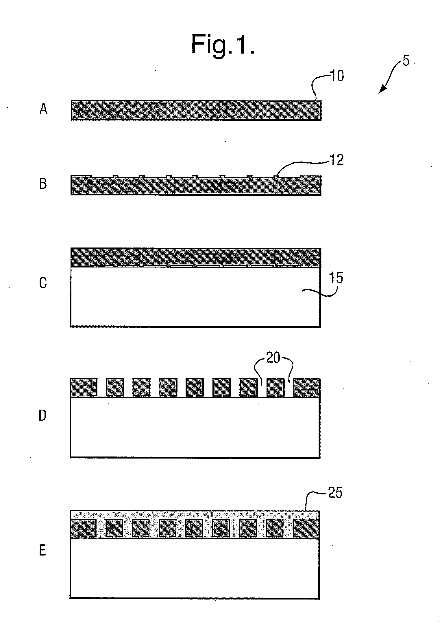
[0078]Referring first to FIG. 1, there is schematically shown therein the various steps (A to E) of a method 5 of fabrication of new mushroom-headed adhesive microstructures in accordance with a first embodiment of the invention.
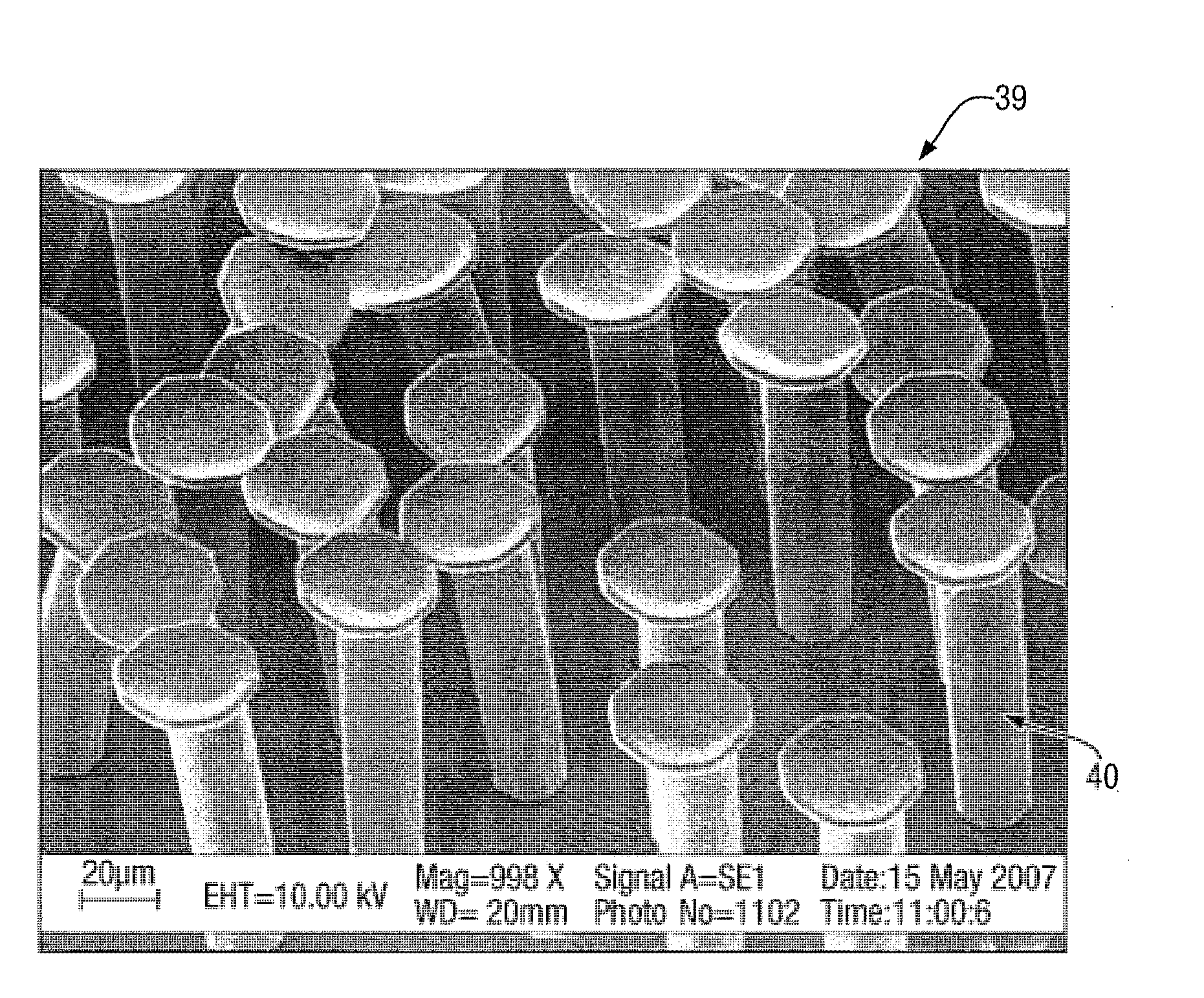
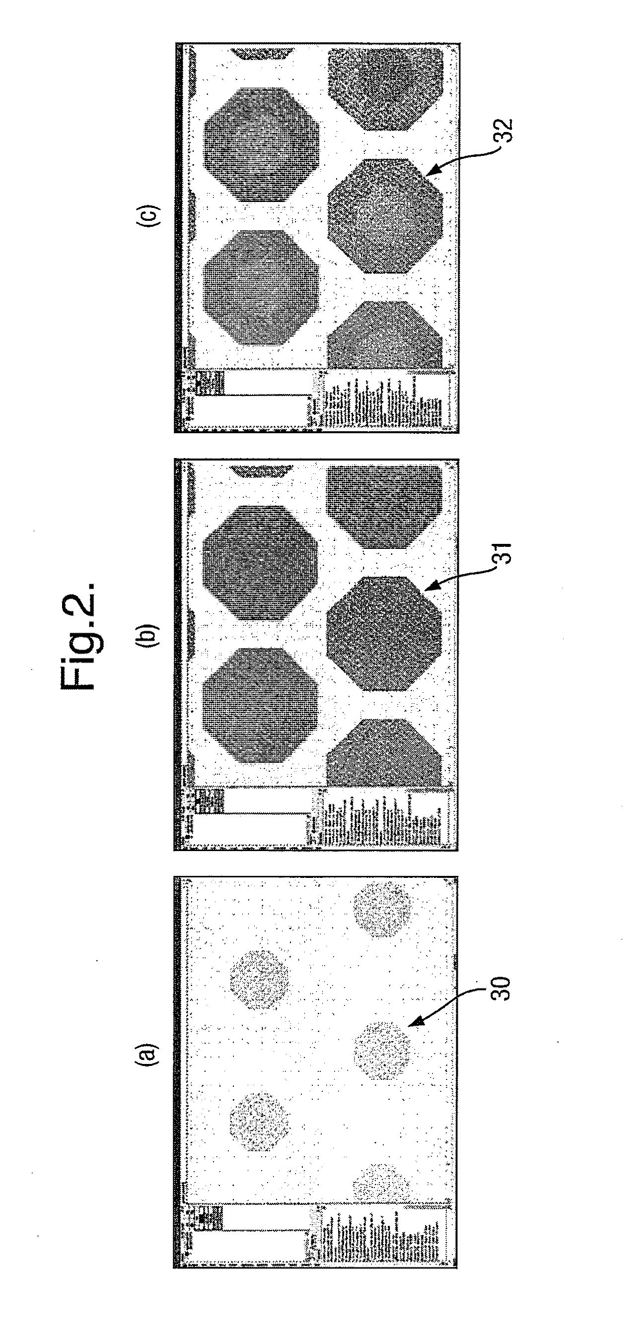
[0079]Two masks (not shown in FIG. 1) were drawn, one with blanking regions defining stalks of the mushroom-headed structure (in the first instance, 20 μm diameter features were chosen) and the other defining blanking regions of the mushroom-heads (40 μm diameter features chosen). These were patterned in hexagonal arrays to maximise packing density, and had common centres. Both of the masks were patterned over their entire area in order to define approximately 1.2 million hair structures. An example of parts of the mask patterns 30, 31, 32 with these chosen diameters are shown in FIGS. 2a, b and c. A silicon wafer 10 with a thickness which defined the stalk length was obtained (Step A), and the 40 μm mask was then used to pattern o...
second embodiment
Method 2 (Second Embodiment)
[0088]Referring next to one of the steps (step 2.) of FIG. 4, there is schematically shown therein how another method is used to fabricate further new mushroom-headed adhesive microstructures in accordance with a second embodiment of the invention.
[0089]Wafers consisting of a 20 μm thick silicon layer on top of an oxide were obtained. These were patterned using negative versions of existing “coarse” and “fine” masks where, as in method 1 described above, blanking regions now defined the regions between hairs, rather than the hairs themselves. An example of a mask 45 defining the required features is shown in FIG. 6. This gave a series of patterns suitable for producing hairs of diameter between approximately 1 μm and 10 μm over each wafer. As will be readily understood by the man skilled in the art of lithography and etching techniques, the etching was conducted in a standard way (see method 1 etch parameters / procedures) and holes were fabricated through ...
third embodiment
Method 3 (Third Embodiment)
[0090]Referring again to FIG. 4, there is schematically shown therein the various steps (1. to 5.) of another method 55 of fabrication of new adhesive microstructures in accordance with a third embodiment of the invention.
[0091]As shown in FIG. 4, a 100 μm thick silicon wafer 60 is first obtained with shallow 40 μm diameter cylindrical cavities formed on one of its surfaces following the steps A. and B. of the above described method 1 (see FIG. 1). Next, a separate wafer 65 comprising 7 μm thick silicon layer on top of silicon oxide is obtained, and 3 μm diameter cylindrical cavities are then etched into this material extending through the 7 μm thickness of the silicon, following the procedure of the above described method 2 (Step 2.). The two wafers are then attached to each other at a surface 68 in such a way that the formed cavities in the wafers are made to coincide at the surface (Step 3.). We believe that the coincidence step is not critical to worki...
PUM
| Property | Measurement | Unit |
|---|---|---|
| Temperature | aaaaa | aaaaa |
| Temperature | aaaaa | aaaaa |
| Time | aaaaa | aaaaa |
Abstract
Description
Claims
Application Information