ENHANCEMENT MODE GaN HEMT DEVICE AND METHOD FOR FABRICATING THE SAME

a technology of enhanced mode and hemt, which is applied in the direction of semiconductor devices, basic electric elements, electrical equipment, etc., can solve the problems of high gate leakage current, gate reliability risk, and increased manufacturing cost of fabrication

Active Publication Date: 2010-10-14
EFFICIENT POWER CONVERSION CORP
View PDF13 Cites 62 Cited by
  • Summary
  • Abstract
  • Description
  • Claims
  • Application Information

AI Technical Summary

Problems solved by technology

The conventional method of fabrication also increases manufacturing costs.
Another disadvantage is that the highest electric field is located at the p-type GaN material or p-type AlGaN material gate corner toward the drain ohmic contact metal.
This high electric field leads to high gate leakage current and a gate reliability risk.

Method used


Image

  • ENHANCEMENT MODE GaN HEMT DEVICE AND METHOD FOR FABRICATING THE SAME
  • ENHANCEMENT MODE GaN HEMT DEVICE AND METHOD FOR FABRICATING THE SAME
  • ENHANCEMENT MODE GaN HEMT DEVICE AND METHOD FOR FABRICATING THE SAME

Examples


first embodiment

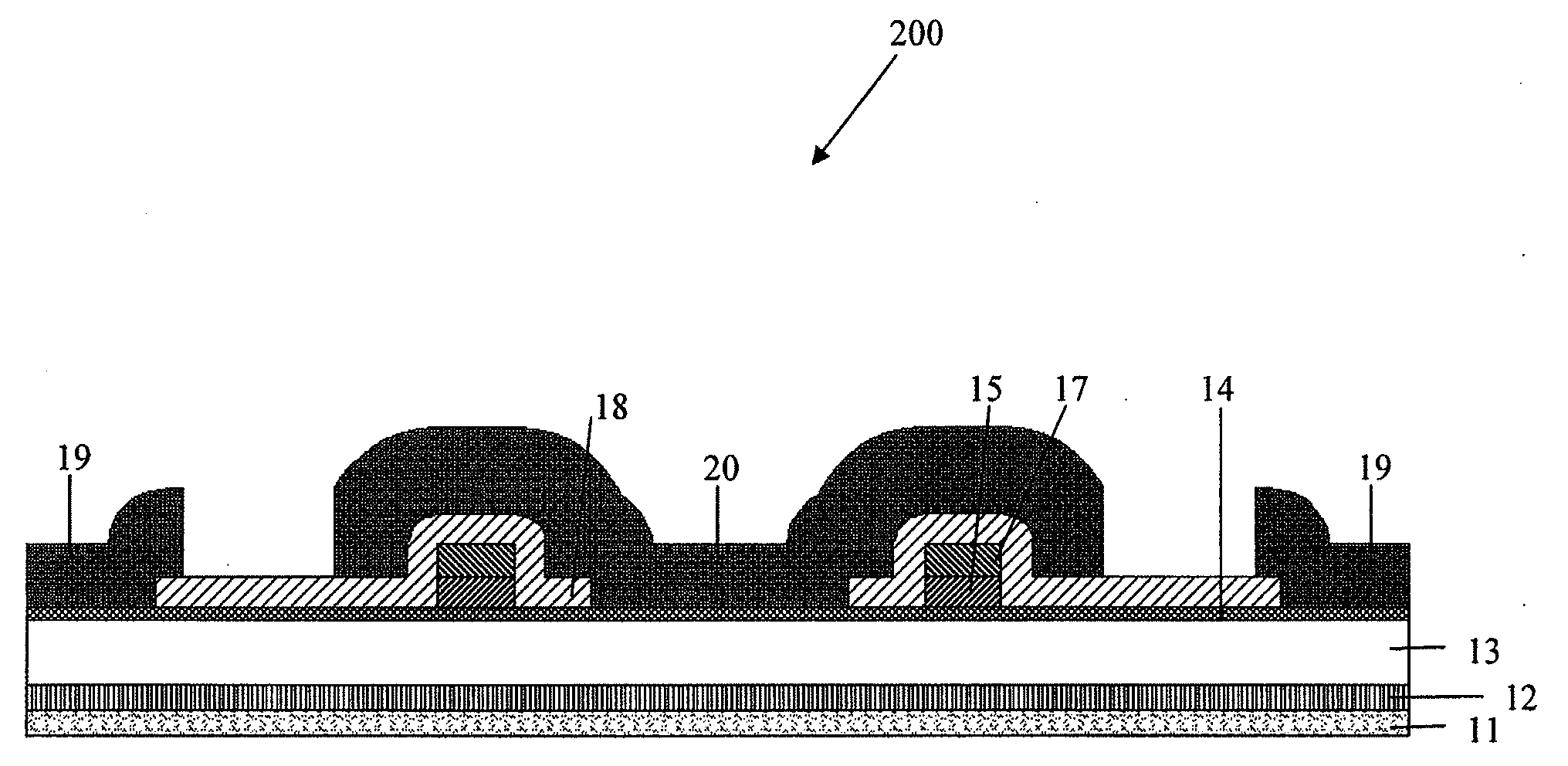
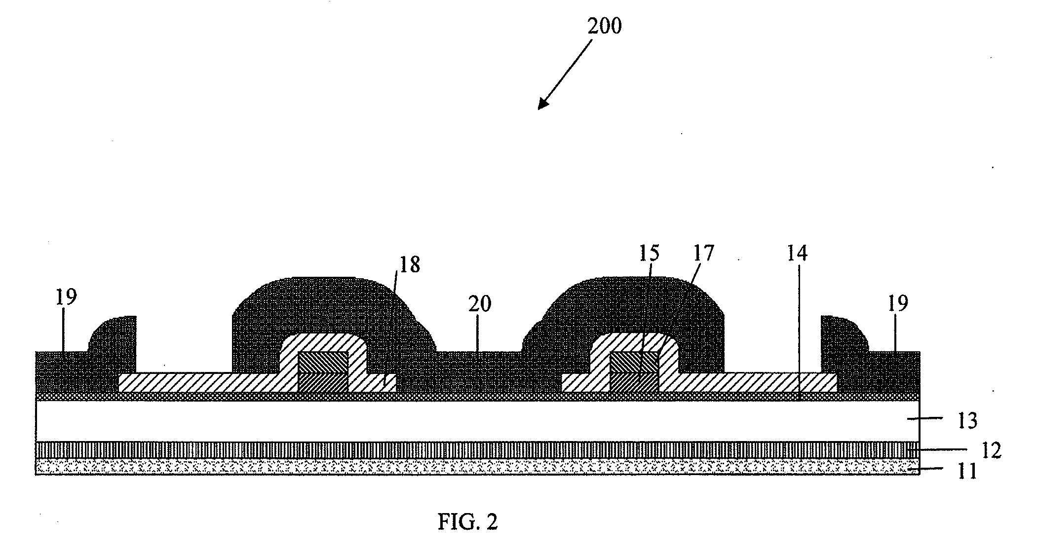
[0023]Referring to FIGS. 2 and 3A-3E, a first embodiment is now described for forming an enhancement mode GaN HEMT device with a self-aligned gate, wherein like reference numbers are used consistently for like features throughout the drawings. FIG. 2 illustrates an enhancement mode GaN HEMT device 200 formed by the method described below with respect to FIGS. 3A-3E, which has a gate metal 17 and a p-type GaN material 15 that are self-aligned. Device 200 includes a silicon substrate 11, transition layers 12, un-doped GaN buffer material 13, un-doped AlGaN barrier material 14, p-type GaN gate layer 15, gate metal 17, dielectric material 18, drain ohmic contact 19, and source ohmic contact 20. The source metal 20 also serves as a field plate that extends over the gate and toward the drain contact. Layers 13, 14, and 15 are made of a III Nitride material. A III Nitride material can be composed of InxAlyGa1−x−yN, where x+y≦1.

[0024]FIG. 3A illustrates the EPI structure of GaN HEMT device ...

second embodiment

[0030]Referring to FIGS. 4 and 5A-5E, the invention is now described. FIG. 4 illustrates an enhancement mode GaN HEMT device 200 formed by the method shown in FIGS. 5A-5E, which results in a gate metal 17, a p-type GaN gate layer 15, and a p-type AlGaN material 21 that are self-aligned. Device 200 in FIG. 4 differs from device 200 of FIGS. 2 and 3A-3E in that it includes an additional layer, namely the layer formed of p-type AlGaN material 21.

[0031]FIG. 5A illustrates the EPI structure, including, from bottom to top, silicon substrate 11, transition layers 12, un-doped GaN buffer material 13, un-doped AlGaN barrier material 14, p-type AlGaN material 21, and p-type GaN material 15. The dimensions and compositions of the various layers are similar to that of the first embodiment. The additional layer of p-type AlGaN material 21 preferably has a thickness of about 20 Å to about 300 Å, and includes Al from about 12 to about 100 percent of the AlGaN material.

[0032]As shown in FIG. 5B, as...

ninth embodiment

[0048]In a ninth embodiment, the p-GaN material 15 is formed by introducing magnesium (Mg) impurities during the growth of the top EPI layer, for example, in FIG. 3A. Magnesium is the most common impurity atom used to create acceptor-rich (p-type) GaN.


PUM

PropertyMeasurementUnit
angleaaaaaaaaaa
angleaaaaaaaaaa
angleaaaaaaaaaa

Abstract

An enhancement-mode GaN transistor and a method of forming it. The enhancement-mode GaN transistor includes a substrate, transition layers, a buffer layer comprised of a III Nitride material, a barrier layer comprised of a III Nitride material, drain and source contacts, a gate III-V compound containing acceptor type dopant elements, and a gate metal, where the gate III-V compound and the gate metal are formed with a single photo mask process to be self-aligned and the bottom of the gate metal and the top of the gate compound have the same dimension. The enhancement mode GaN transistor may also have a field plate made of Ohmic metal, where a drain Ohmic metal, a source Ohmic metal, and the field plate are formed by a single photo mask process.

Description

CROSS REFERENCE TO RELATED APPLICATIONS[0001]This application claims priority from U.S. Provisional Application No. 61 / 167,777, filed on Apr. 8, 2009, which is hereby incorporated by reference in its entirety.FIELD OF THE INVENTION[0002]The present invention relates to the field of enhancement mode gallium nitride (GaN) high electron mobility transistor (HEMT) devices. In particular, the invention relates to a method and apparatus for providing an enhancement type HEMT device.BACKGROUND OF THE INVENTION[0003]Gallium nitride (GaN) semiconductor devices are increasingly desirable for power semiconductor devices because of their ability to carry large current and support high voltages. Development of these devices has generally been aimed at high power / high frequency applications. Devices fabricated for these types of applications are based on general device structures that exhibit high electron mobility and are referred to variously as heterojunction field effect transistors (HFET), h...

Claims


Application Information

Patent Timeline
Patent Type & Authority Applications(United States)
IPC IPC(8): H01L29/778H01L21/335
CPCH01L29/1066H01L29/2003H01L29/778H01L29/66462H01L29/7786H01L29/402H01L21/18
Inventor LIDOW, ALEXANDERBEACH, ROBERTNAKATA, ALANACAO, JIANJUNZHAO, GUANG YUAN
Owner EFFICIENT POWER CONVERSION CORP
Why Eureka
Try Eureka