

Electronic device including electronic part and wiring substrate
a technology of electronic parts and wiring substrates, applied in the direction of short-circuit testing, instruments, and the details of semiconductor/solid-state devices, can solve the problems of affecting the life of the device, affecting the performance of the device, so as to achieve the effect of long li
- Summary
- Abstract
- Description
- Claims
- Application Information
AI Technical Summary
Benefits of technology
Problems solved by technology
Method used
Image

Examples
first embodiment
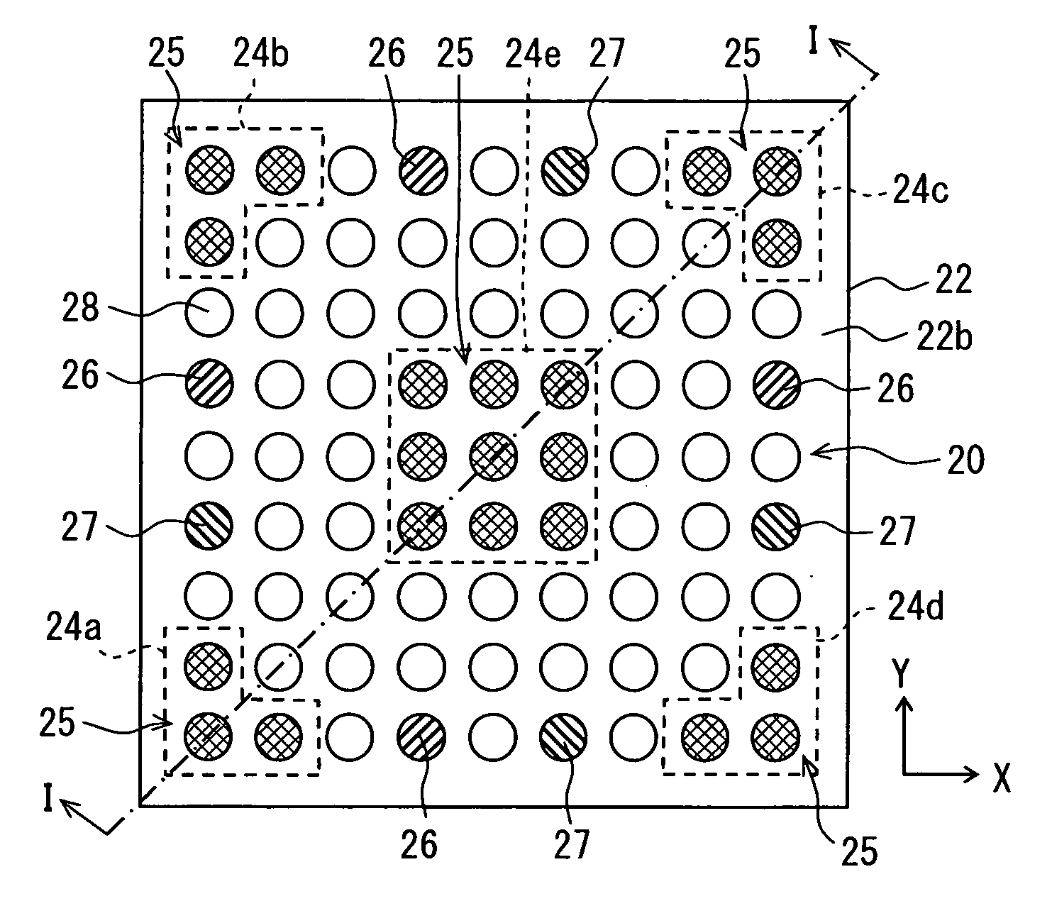
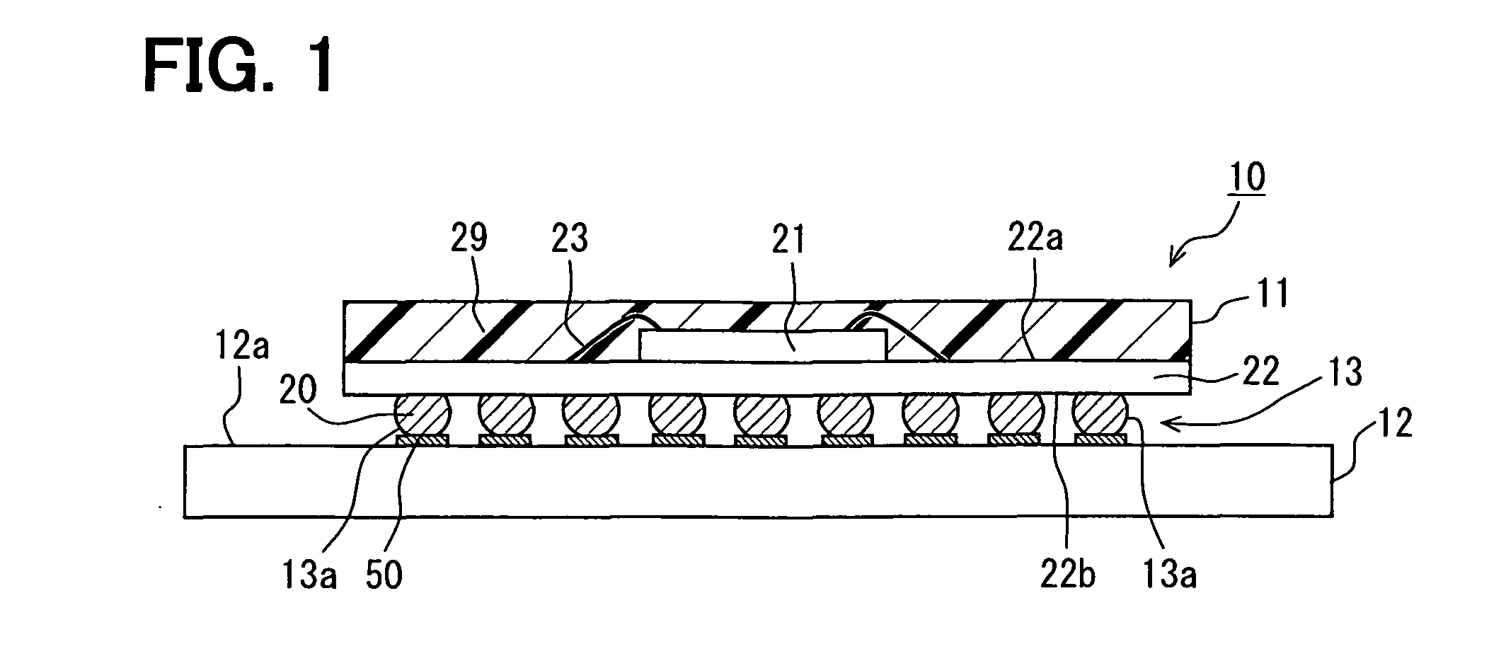
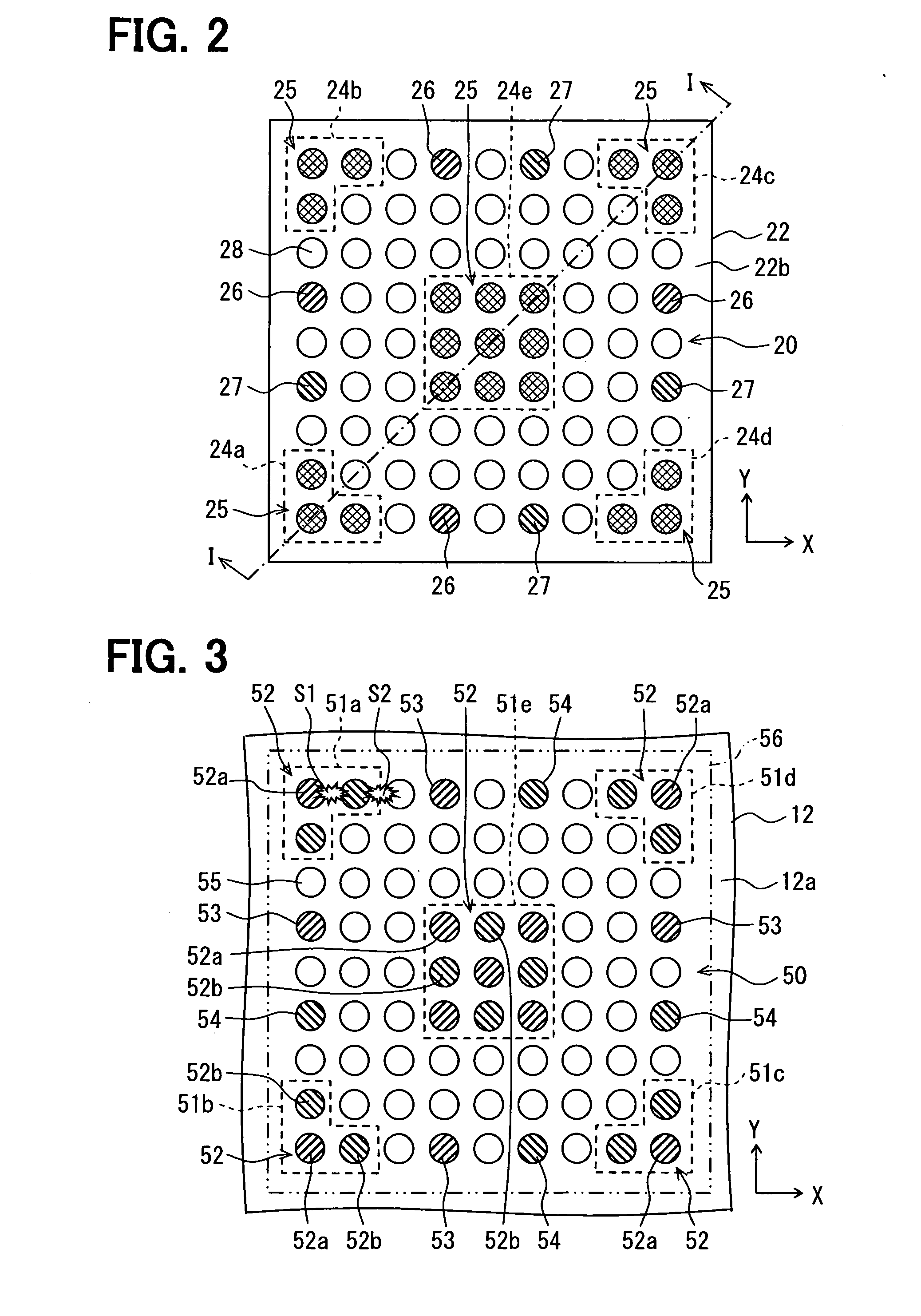
[0040]An electronic device 10 according to a first embodiment of the present invention will be described with reference to FIG. 1-FIG. 3.
[0041]As shown in FIG. 1, the electronic device 10 includes an electronic part 11 and a wiring substrate 12. The electronic part 11 has a plurality of solder bumps 20. The wiring substrate 12 has a plurality of lands 50. The solder bumps 20 are mechanically and electrically coupled with the lands 50, respectively.
[0042]The electronic part 11 is so-called semiconductor package (IC). The electronic part 11 includes a semiconductor chip 21 and a rewiring substrate 22. The rewiring surface includes a first surface 22a and a second surface 22b being opposite each other. The semiconductor chip 21 is fixed on the first surface 22a of the rewiring substrate 22. The solder bumps 20 are arranged on the second surface 22b of the rewiring substrate 22.
[0043]The semiconductor chip 21 includes a semiconductor substrate, elements, and a wiring layer. The substrat...
second embodiment
[0065]An electronic device 10 according to a second embodiment of the present invention will be described with reference to FIG. 4 and FIG. 5.
[0066]Because the electronic device 10 according to the present embodiment has many portions in common with the electronic device 10 according to the first embodiment, a description of the common portions will be omitted and different portions will be mainly described. Components of the electronic device 10 according to the present embodiment have the same reference numbers as similar components of the electronic device 10 according to the first embodiment.
[0067]In the present embodiment, in nonfunctional bumps 25 and nonfunctional lands 52 that form nonfunctional connection portions 13a, the nonfunctional bumps 25 includes power source bumps 25a fixed to the power source potential and ground bumps 25b fixed to the ground potential as shown in FIG. 4. The power source bumps 25a and the ground bumps 25b are coupled with wires of the rewiring su...
third embodiment
[0071]An electronic device 10 according to a third embodiment of the present invention will be described with reference to FIG. 6 to FIG. 9.
[0072]Because the electronic device 10 according to the present embodiment has many portions in common with the electronic devices 10 according to the above-described embodiments, a description of the common portions will be omitted and different portions will be mainly described. Components of the electronic device 10 according to the present embodiment have the same reference numbers as similar components of the electronic device 10 according to the above-described embodiments.
[0073]The electronic device 10 includes an electronic part 11, and a wiring substrate 12. The electronic part 11 has a plurality of solder bumps 20. The wiring substrate 12 has a plurality of lands 50. The solder bumps 20 are mechanically and electrically coupled with the lands 50, respectively. As shown in FIG. 6, the solder bumps 20 are arranged in a 9×9 matrix in the ...
PUM
 Abstract
Description
Claims
Application Information