Magnetic detection of back-side layer

a backside layer and magnetic detection technology, applied in the field of integrated circuits, can solve the problems of partial removal or complete removal and achieve the effect of preventing the damage of the magnetically able region

Active Publication Date: 2010-11-11
NXP BV
View PDF8 Cites 17 Cited by
  • Summary
  • Abstract
  • Description
  • Claims
  • Application Information

AI Technical Summary

Benefits of technology

[0012]The effect of the features of the integrated circuit according to the invention is that a very simple construction is achieved. All what is needed is a magnetizable region on the second side and at least one magnetic field sensor on the first side of the substrate. Above that, these additional features can be provided on the substrate using deposition processing techniques which enables a strongly miniaturized solution which is, because of its reduced dimensions well suitable for being used in bank cards. An attempt to remove the integrated circuit according to the invention from its environment (e.g. a bank card or a package) may result in the magnetizable region getting damaged (partially removed) or even completely removed. In case the magnetizable region has been magnetized (such that it has a magnetic moment that results in a magnetic field detectable at the location of the at least one magnetic field sensor) this damaging or removal may be detected by the at least one magnetic field sensor which provides a first level of security against external attack.
[0025]The first group and the second group of embodiments may be combined. In that case the magnetic field at the location of the electronic circuit has both a lateral magnetic field component as well as a vertical magnetic field component. In that case a combination of a magnetic field sensor that is sensitive to the lateral magnetic field component and a magnetic field sensor that is sensitive to the vertical magnetic field component may be used. In further embodiments this feature is exploited to create more variation in read-out of the magnetic field sensors.
[0028]Preferably, the transistor is a bipolar transistor with an emitter, base and collector. In that case, the collector is split into a first and second collector region each carrying a detection current. Herein, the first and second collector regions, the base region, and the emitter region are positioned with respect to each other such that, in operation, a part of an emitter current that traverses the base region is distributed over the first and second collector regions obtaining the first and the second detection current. The use of this bipolar transistor as magnetic field sensor with a split-collector configuration enables a high linearity and a high sensitivity.
[0037]The magnetic field sensor in this embodiment effectively constitutes a 2-in-1 magnetic field sensor which advantageously features a 2-dimensional magnetic field direction measurement, which allows for more possible read-outs of the magnetic field sensor given a certain magnetization pattern of the magnetizable region. A first magnetic field component is measured by the first and second collector regions, perpendicular to the current plane, and a second magnetic field component is measured by the third and fourth collector regions, in a direction perpendicular to the further current plane.
[0043]Preferably in the earlier mentioned embodiments having a bipolar magnetotransistor, the electronic circuit at least comprises CMOS circuitry. CMOS circuitry is fully compatible with triple-well technology and this embodiment thus features easy integration of the magnetotransistor (which is compatible with triple-well technology) with the electronic circuit. This particularly allows the integration of the sensor with an A / D converter. In that manner, the distance for transmitting analog signals within the integrated circuit can be kept short. That is relevant in order to detect small differences in detection currents.

Problems solved by technology

An attempt to remove the integrated circuit according to the invention from its environment (e.g. a bank card or a package) may result in the magnetizable region getting damaged (partially removed) or even completely removed.

Method used


Image

  • Magnetic detection of back-side layer
  • Magnetic detection of back-side layer
  • Magnetic detection of back-side layer

Examples


first embodiment

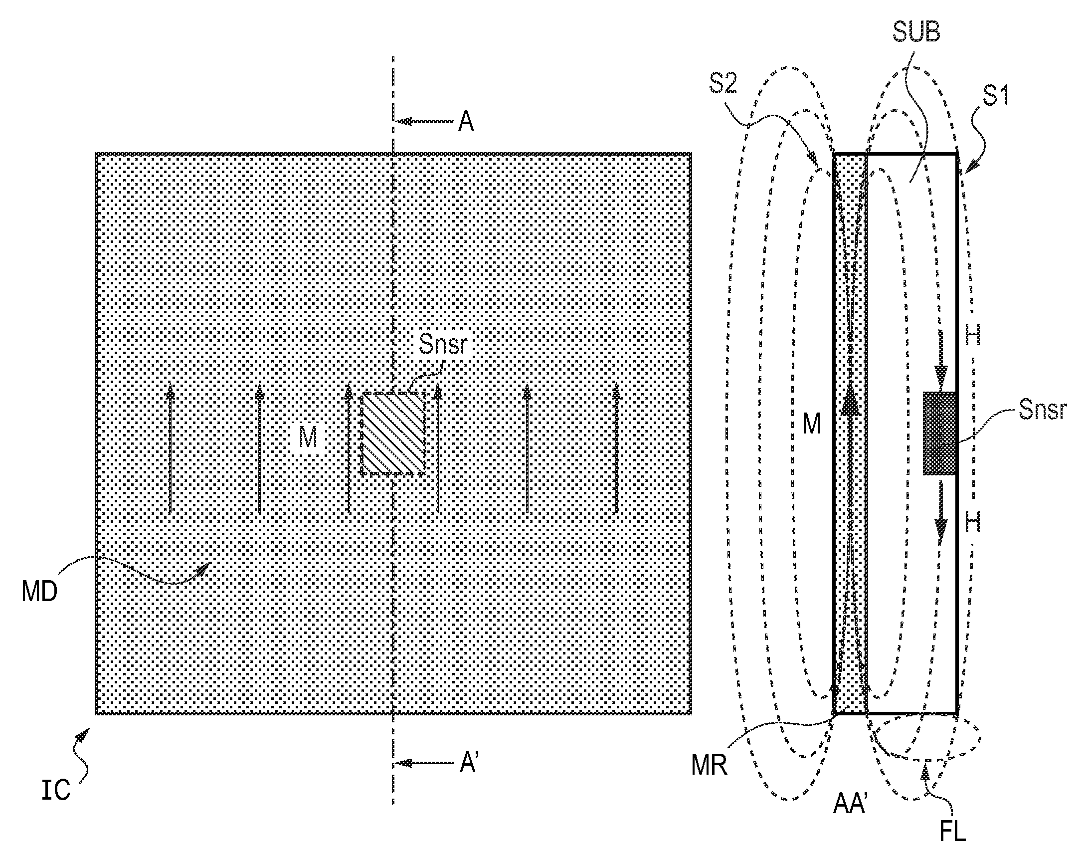
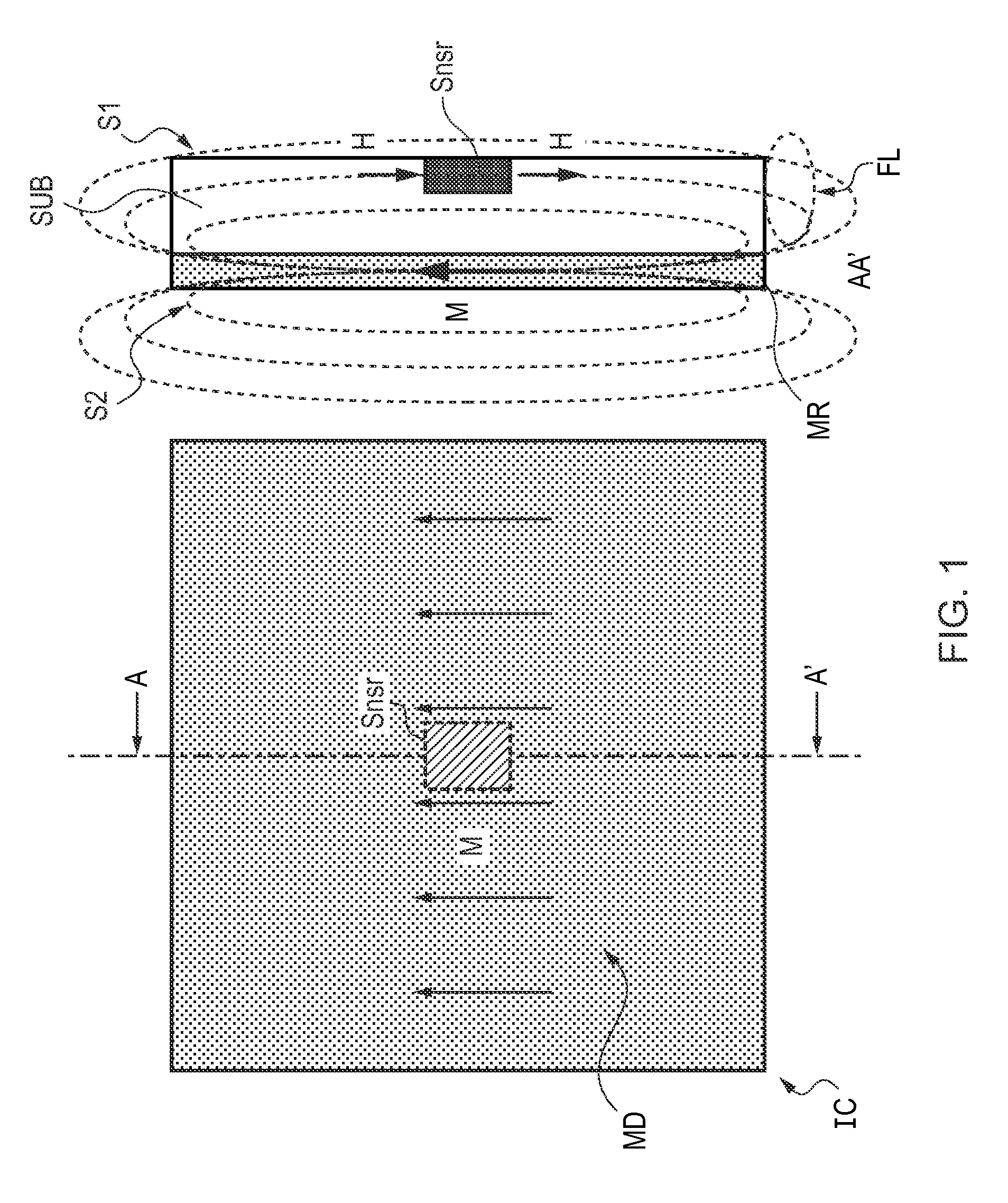
[0081]FIG. 1 shows a schematic top-view and a schematic cross-sectional view of an integrated circuit in accordance with the invention. The cross-sectional view on the right-hand side of the Figure is taken at line AA′ in the top-view on the left-hand side of the Figure. The integrated circuit IC comprises a substrate SUB having a first side S1 (front-side) and a second side S2 (back-side). On the first side S1 an electronic circuit (not shown) is provided. The electronic circuit comprises a magnetic field sensor Snsr. On the second side S2 of the substrate SUB a magnetizable region MR has been provided by means of a wafer-level type deposition processing step.

[0082]A magnetizable material like neodymium-iron-boron (NdFeB) or cobalt-platinum (CoPt) can be deposited on the second side S2 of the substrate SUB by means of a sputtering step. This can be done from a homogeneous target of these materials in a DC or RF type sputtering system in Argon (Ar) at a pressure of typically 1-20 mT...

second embodiment

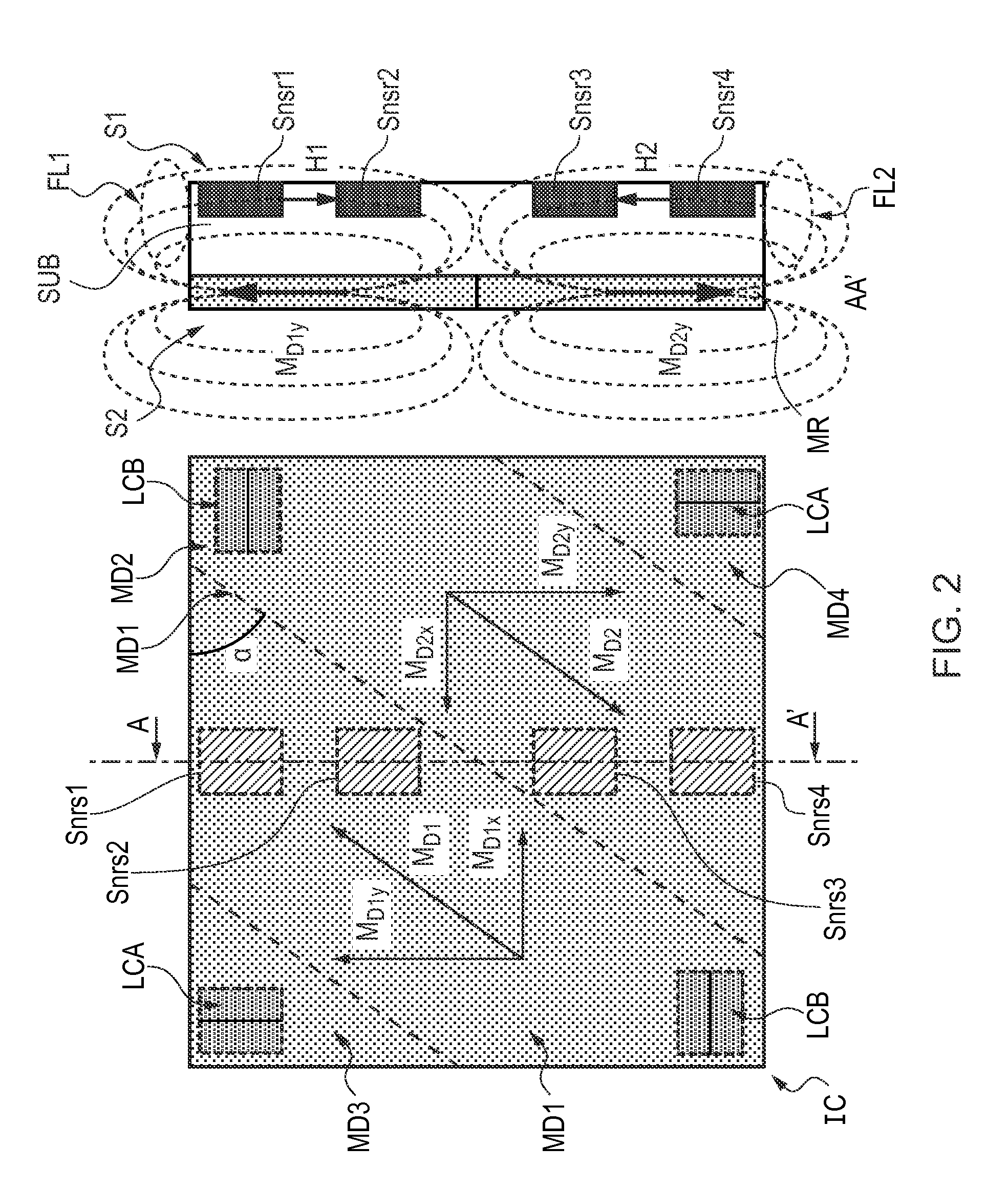
[0087]FIG. 2 shows a schematic top-view and a schematic cross-sectional view of an integrated circuit in accordance with the invention. The cross-sectional view on the right-hand side of the Figure is taken at line AA′ in the top-view on the left-hand side of the Figure. In this embodiment of the integrated circuit IC the magnetic region MR is provided with four magnetization domains MD1, MD2, MD3, MD4, wherein each magnetization domain has a different magnetic moment M. A first one MD1 of the magnetization domains has a first magnetic moment MD1 in a first direction, and a second one MD2 of the magnetization domains has a second magnetic moment MD2 in a second direction opposite to the first direction. Between the first magnetization domain MD1 and the second magnetization domain MD2 there is an interface MDI having a varying direction of magnetization. This interface is also called a domain wall. In this example the interface MDI follows a straight line that makes an angle α with ...

third embodiment

[0133]FIG. 10 shows a schematic top-view of a magnetic field sensor which may be used in the integrated circuit of the invention. The embodiments illustrated in FIGS. 6 and 7 may be extended towards two-dimensional field measuring capabilities by adding another pair of collector regions for enabling the measurement of a further magnetic field component By in a direction parallel to the first side of the substrate. Effectively, a bipolar transistor having 4 collector terminals (CL1, CL2, CL3, CL4) is achieved instead of two. Preferably, the structure is designed symmetrically as illustrated in FIG. 10, which means that the current plane and the further current plane are perpendicular with respect to each other.

[0134]In the embodiment as illustrated in FIG. 10, during operation of the magnetic field sensor, collector regions C1 and C3 measure a first magnetic field component By, wherein the following formula may be derived:

ΔIC13=K′·By·IE·μHn.

wherein ΔIC13 is the difference in collecto...


PUM


Abstract

The invention relates to an integrated circuit comprising a substrate having a first side and a second opposing side. An electronic circuit (EC) is provided at the first side (S1) of the substrate, wherein the electronic circuit (EC) comprises at least one magnetic field sensor (Snsr, Snsr1, Snsr2, Snsr3, Snsr4). The integrated circuit further comprises a magnetizable region (MR) provided on the second side (S1) of the substrate (SUB) by using a wafer-level type deposition processing step. The magnetic moment of the magnetizable region (MR) is configurable for generating a magnetic field (H1, H2) detectable at the location of the at least one magnetic field sensor Snsr3 (Snsr, Snsr1, Snsr2, Snsr3, Snsr4). The integrated circuit constitutes a very simple construction and enables a strongly miniaturized solution which is, because of its reduced dimensions well suitable for being used in bank cards. An attempt to remove the integrated circuit according to the invention from its environment (e.g. a bank card) may result in the magnetizable region (MR) getting damaged (partially removed) or even completely removed. The invention provides a first level of security against external attack. Embodiments of the invention provide higher security levels. Various magnetic field sensors are illustrated which may be advantageously integrated in the integrated circuit. The invention also relates to a card provided with such integrated circuit. The card in accordance with the invention is more secure. The invention further relates to a method of initializing such integrated circuit and a method of checking the authenticity of such integrated circuit.

Description

FIELD OF THE INVENTION[0001]The invention relates to an integrated circuit in accordance with claim 1, a card provided with such integrated circuit, a method of initializing such integrated circuit, and a method of checking the authenticity such integrated circuit.BACKGROUND OF THE INVENTION[0002]Integrated circuits (IC's) for applications such as smartcards, RFID tags, Pay-TV chips often contain a secret security key and carry out secret functions. The IC needs to be secure against attacks from the outside which aim at retrieving data there from. IC's may be subjected to both front-side as well as back-side attacks. In this description the “front-side” of a semiconductor device is defined as the side of the semiconductor device on which circuitry is provided. This side is also being referred to as the “first side of the substrate” in this description. Likewise, the“back-side” of the semiconductor device is defined as the side opposite to the front-side and this side is also being r...

Claims


Application Information

Patent Timeline
Patent Type & Authority Applications(United States)
IPC IPC(8): G01R33/02
CPCH01L23/57H01L2924/3011H01L2224/73265H01L2924/1305H01L2924/12032H01L2224/48091H01L2224/48247H01L2924/13091H01L2924/30107H01L2924/3025H01L2924/00014H01L2924/00
Inventor ZIEREN, VICTORWOLTERS, ROBERTUS A. M.
Owner NXP BV
Why Eureka
Try Eureka