Electron emitting element, electron emitting device, light emitting device, image display device, air blowing device, cooling device, charging device, image forming apparatus, and electron-beam curing device

Active Publication Date: 2010-11-25
SHARP KK
View PDF21 Cites 22 Cited by
  • Summary
  • Abstract
  • Description
  • Claims
  • Application Information

AI Technical Summary

Benefits of technology

[0011]where Ie [A/cm2] is electron emission current per unit area during voltage application and R is element resistance [Ω·cm2] per unit area, the element resistance being obtained by dividing (a) the voltage applied between the electrode substrate and the thin-film electrode during the voltage application by (b) current in element per unit area which current flows between the electrode substrate and the thin-film electrode during the voltage application, and where α is not less than 2.0×10⁻⁶, and the electron emission current Ie is not less than 1.0×10⁻⁹.
[00

Problems solved by technology

This causes a problem of breakdown of the electron emitting element due to sputtering.
Ozone is harmful to human bodies, and oxidizes various substances because of its strong oxidizing power.
This causes a problem in

Method used


Image

  • Electron emitting element, electron emitting device, light emitting device, image display device, air blowing device, cooling device, charging device, image forming apparatus, and electron-beam curing device
  • Electron emitting element, electron emitting device, light emitting device, image display device, air blowing device, cooling device, charging device, image forming apparatus, and electron-beam curing device
  • Electron emitting element, electron emitting device, light emitting device, image display device, air blowing device, cooling device, charging device, image forming apparatus, and electron-beam curing device

Examples


embodiment 1

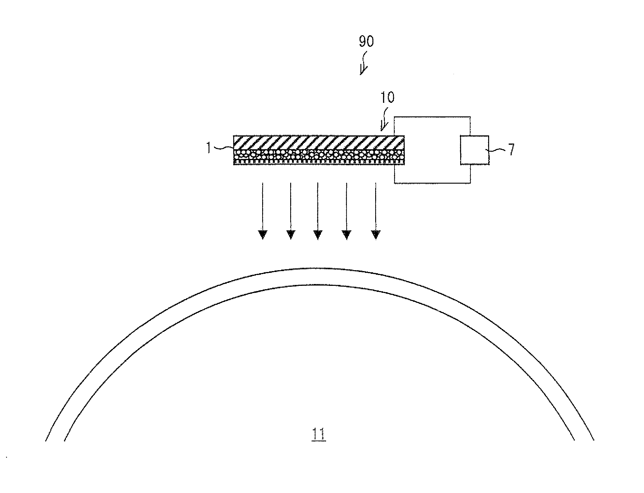
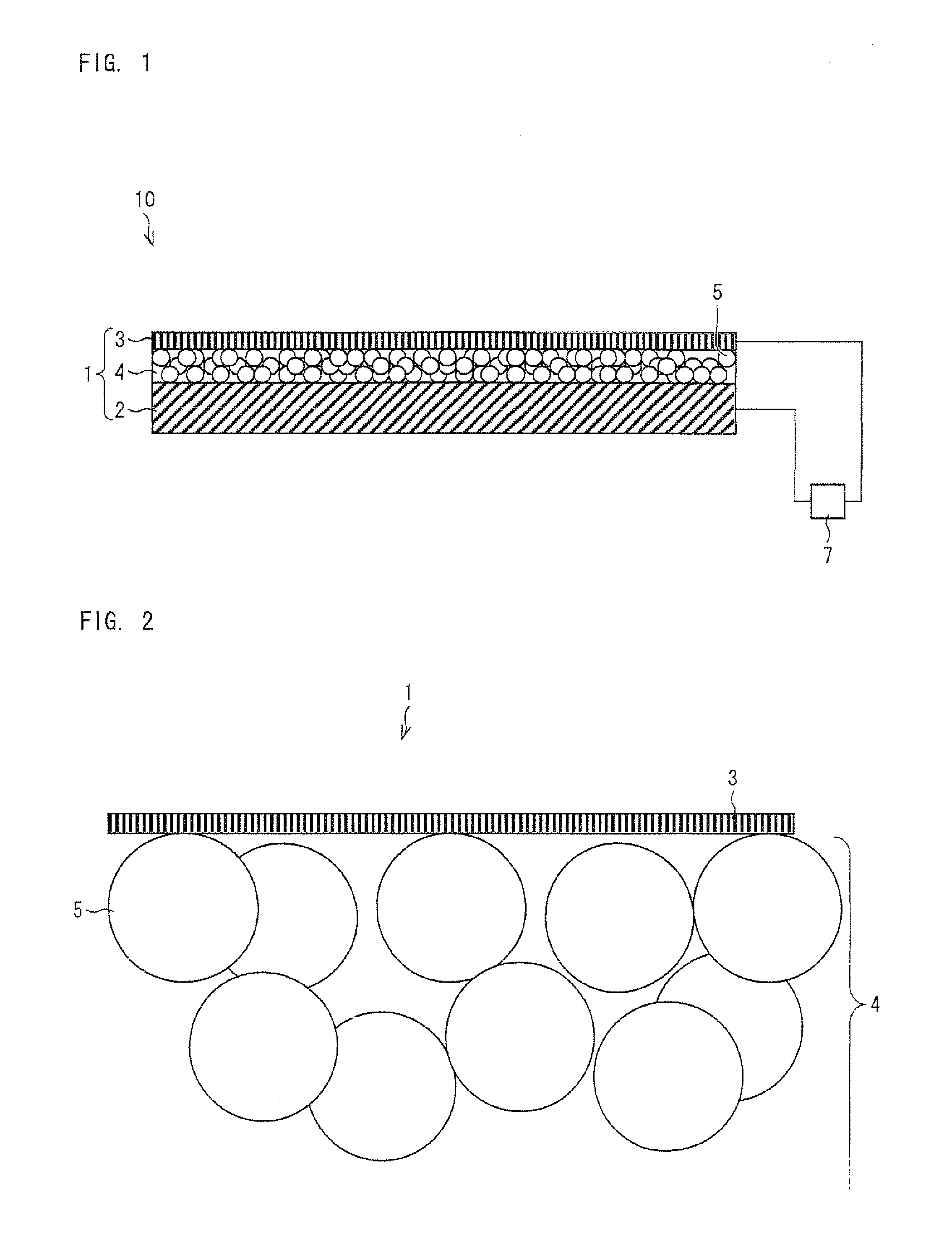
[0054]FIG. 1 is a schematic view illustrating an arrangement of an electron emitting device 10 including an electron emitting element 1 according to one embodiment of the present invention. As shown in FIG. 1, the electron emitting device 10 includes an electron emitting element 1 according to one embodiment of the present invention, and a power supply 7. The electron emitting element 1 includes: an electrode substrate 2 as a bottom electrode; a thin-film electrode 3 as an upper electrode; and an electron acceleration layer 4 sandwiched therebetween. Further, the electrode substrate 2 and the thin-film electrode 3 are connected to the power supply 7, so that a voltage can be applied between the electrode substrate 2 and the thin-film electrode 3 which are provided so as to face each other.

[0055]The electron emitting element 1 applies a voltage between the electrode substrate 2 and the thin-film electrode 3 so that current flows through the electron acceleration layer 4 provided betw...

example 1

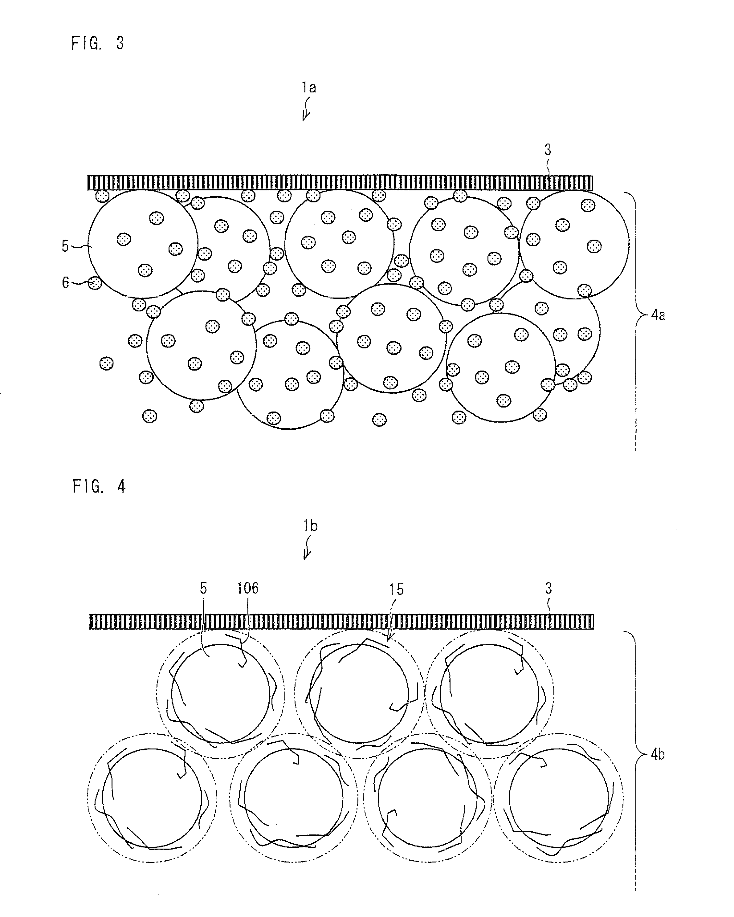
[0132]First, 3.0 g of toluene was supplied as a solvent into a 10 mL reagent bottle. Then, 0.50 g of spherical silica fine particles EP-C413 (manufactured by Cabot Corporation), having an average particle diameter of 50 nm were added to the toluene. Subsequently, the reagent bottle was set in an ultrasonic dispersion device so that the silica fine particles serving as the insulating fine particles 5 were dispersed. Subsequently, 0.12 g of silver nanoparticles (average particle diameter: 10 nm (inclusive of a thickness of 1 nm of an alcoholate insulating coating film), manufactured by Applied Nanoparticle Laboratory Co.) were further added as the conductive fine particles 6. Then, the reagent bottle was set in the ultrasonic dispersion device again so that a dispersion solution was obtained. A ratio of the conductive fine particles 6 with respect to a total mass of the added particles was approximately 20%.

[0133]Next, the dispersion solution thus obtained was dropped on a 30-mm squar...

example 2

[0140]A fine particle dispersion solution in which silica fine particles serving as the insulating fine particles 5 were dispersed was produced as follows. First, 3 mL of toluene was supplied as a solvent into a 10 mL reagent bottle. Then, 0.03 g of AJISPER PB821 (manufactured by Ajinomoto Fine-Techno Co., Inc.) serving as the basic dispersant (basic functional copolymer) 106 was added to the toluene. Subsequently, the reagent bottle was set in an ultrasonic dispersion device so that the AJISPER PB821 was dispersed. After that, 0.25 g of silica particles were added thereto, and the reagent bottle was again set to the ultrasonic dispersion device so that the silica particles were dispersed. The silica particles are fumed silica C413 (manufactured by Cabot Corporation) having a diameter of 50 nm, and surfaces of the silica fine particles are subjected to a hexamethyldisilazane treatment. The reagent bottle was processed in the dispersing device for about 10 minutes, so that the silica...


PUM


Abstract

The present invention provides an electron emitting element which has good energy efficiency and which is capable of controlling a value of current flowing in an electron acceleration layer and an amount of emitted electrons by adjusting a resistance value of the electron acceleration layer and an amount of generated ballistic electrons. An electron emitting element 1 includes an electron acceleration layer 4 including a fine particle layer containing insulating fine particles. In the electron emitting element 1,
Ie=α·R−0.67
    • where Ie [A/cm2] is electron emission current per unit area during the voltage application and R is element resistance [Ω·cm2] per unit area, the element resistance being obtained by dividing (a) a voltage applied between the electrode substrate 2 and the thin-film electrode 3 during the voltage application by (b) current in element per unit area which current flows between the electrode substrate 2 and the thin-film electrode 3 during the voltage application, and where α is not less than 2.0×10⁻⁶, and the electron emission current Ie is not less than 1.0×10⁻⁹.

Description

[0001]This Nonprovisional application claims priority under 35 U.S.C. §119(a) on Patent Application No. 2009-121460 filed in Japan on May 19, 2009, the entire contents of which are hereby incorporated by reference.TECHNICAL FIELD[0002]The present invention relates to an electron emitting element for emitting electrons by application of a voltage, an electron emitting device, a light emitting device, an image display device, an air blowing device, a cooling device, a charging device, an image forming apparatus, and an electron-beam curing device, each of which uses the electron emitting element.BACKGROUND ART[0003]A Spindt-type electrode and a carbon nanotube electrode (CNT) have been known as conventional electron emitting elements. Applications of such conventional electron emitting elements to, for example, the field of Field Emission Display (FED) have been studied. Such electron emitting elements are caused to emit electrons by tunnel effect resulting from formation of an intens...

Claims


Application Information

Patent Timeline
IPC IPC(8): G03G15/02H01J1/02H05B41/00H01T23/00
CPCH01J1/312H01J31/127G03G15/02B82Y10/00H01J2201/3125
Inventor HIRAKAWA, HIROYUKINAGAOKA, AYAEIMURA, YASUOIWAMATSU, TADASHI
Owner SHARP KK
Why Eureka
Try Eureka