Asymmetrically recessed high-power and high-gain ultra-short gate HEMT device

Active Publication Date: 2010-12-02
BAE SYST INFORMATION & ELECTRONICS SYST INTERGRATION INC
View PDF5 Cites 29 Cited by
  • Summary
  • Abstract
  • Description
  • Claims
  • Application Information

AI Technical Summary

Benefits of technology

[0029]There is therefore a balance between the recess design and the double-doping scenario such that gate length, lateral scaling, vertical scaling and channel design operate in concert to provide for the much improved performance of the high electron mobility transistor.
[0030]The net result of the above is that one can fabricate an HEMT with an ultra-high gain at 110 GHz and is capable of operating at 340 GHz and bey

Problems solved by technology

It is noted that for transistor amplifiers, gain drops as frequency increases such that high power devices design

Method used


Image

  • Asymmetrically recessed high-power and high-gain ultra-short gate HEMT device
  • Asymmetrically recessed high-power and high-gain ultra-short gate HEMT device
  • Asymmetrically recessed high-power and high-gain ultra-short gate HEMT device

Examples


Example

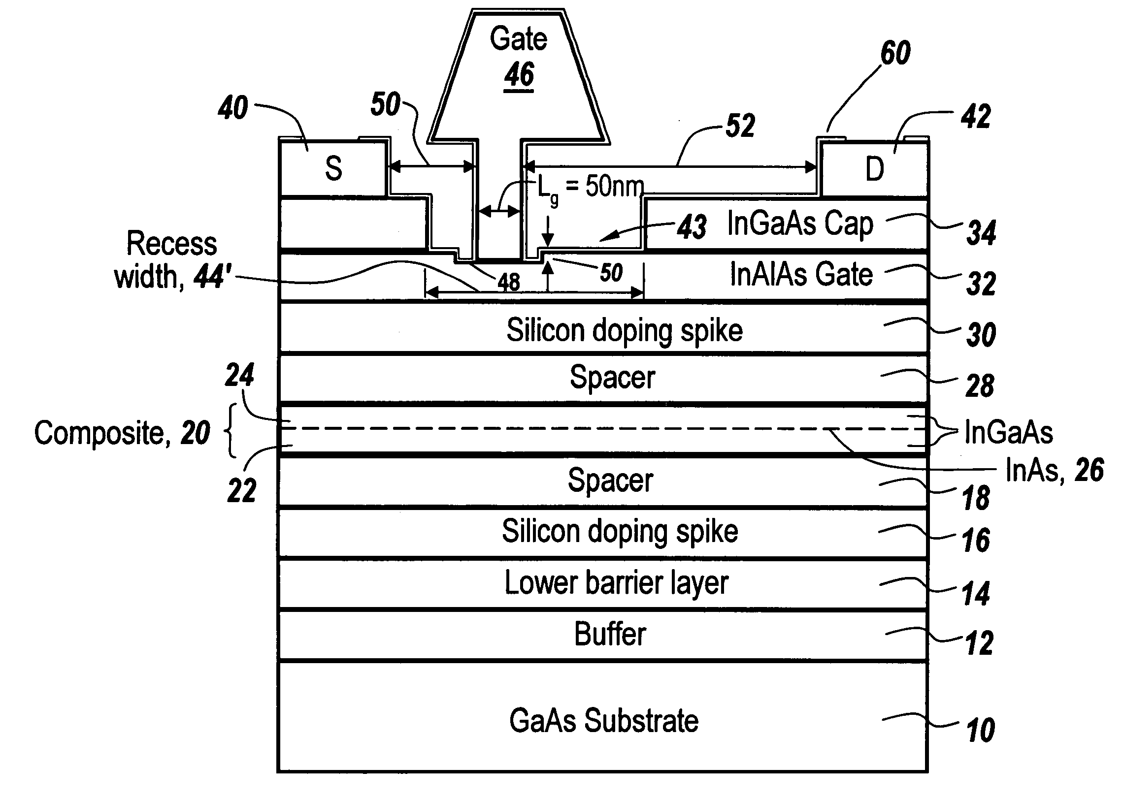
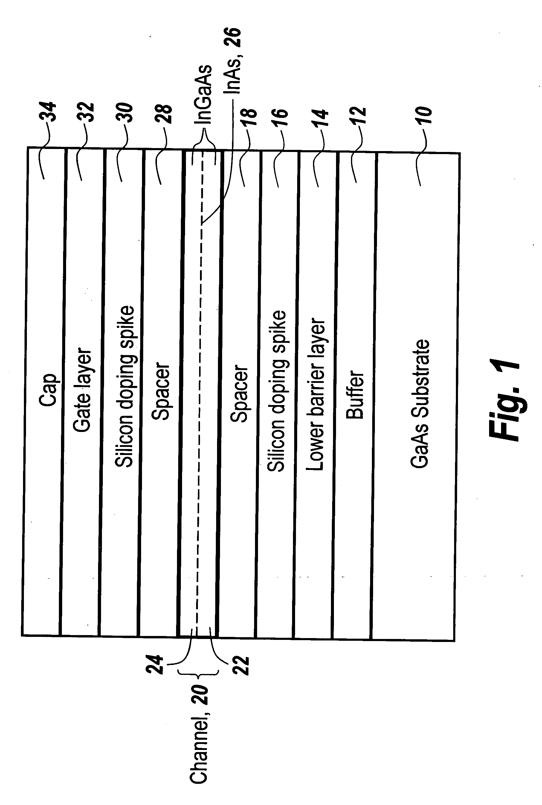
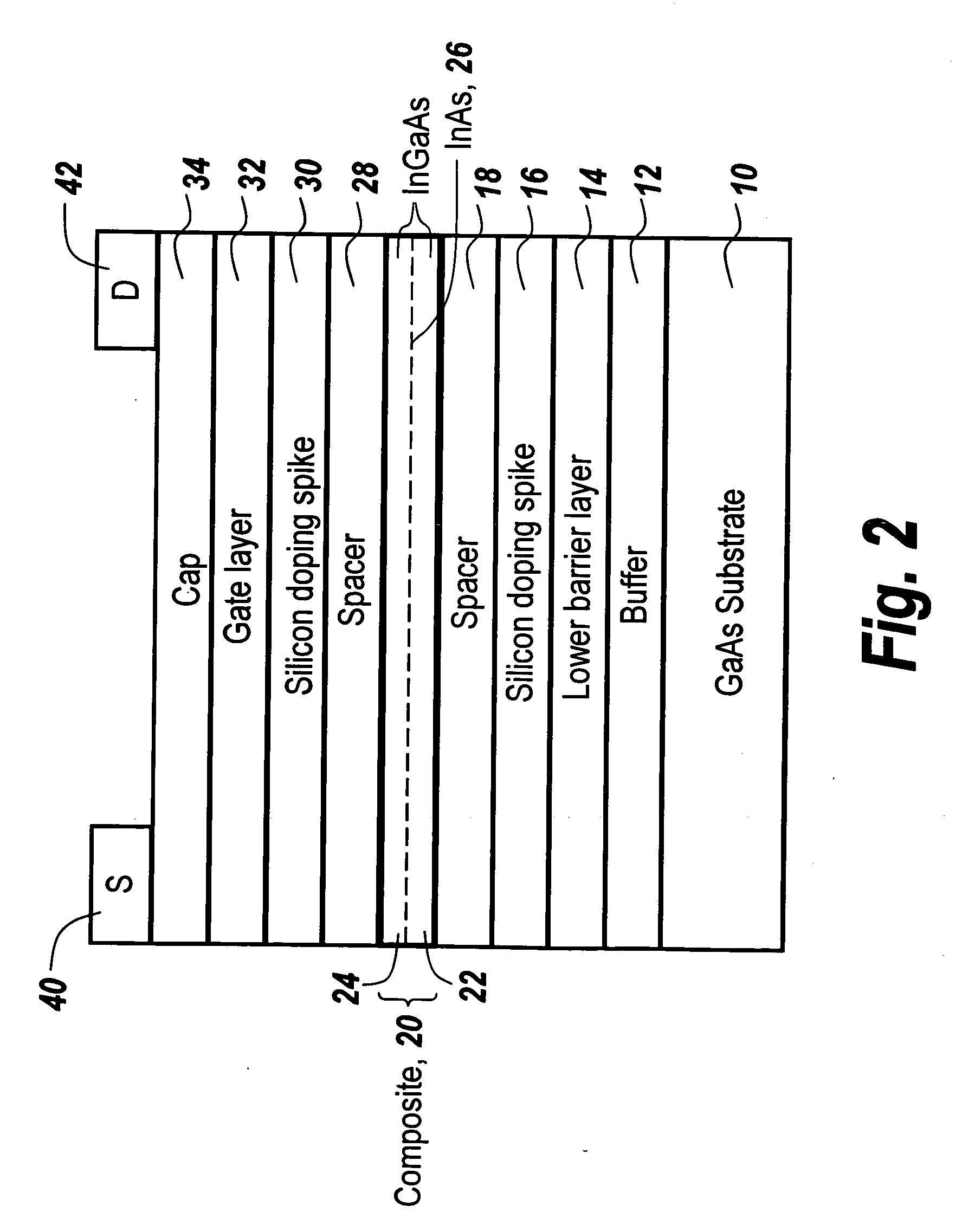
[0042]Referring now to FIG. 1, in the subject invention the epitaxial structure which leads to the improved device includes a gallium arsenide substrate 10 on top of which is provided a buffer 12, in one form an InAlAs buffer. On top of the buffer is deposited a lower barrier layer 14.

[0043]The first of the two silicon doping spike layers is shown as a lower silicon doping spike layer 16 on top of which is a spacer 18, in one embodiment an InAlAs spacer.

[0044]The composite channel 20 includes a bottom indium gallium arsenide layer 22 and an upper indium gallium arsenide layer 24 having an embedded indium arsenide layer 26 which is relatively thin compared to the overall dimensions of the channel layer. In one embodiment the indium arsenide layer is 2 nanometers in thickness, with the indium gallium arsenide layers surround it each being of 2 nanometers in thickness, making the overall channel 6 nanometers thick.

[0045]On top of channel 20 is a spacer 28, in one embodiment an InAlAs s...


PUM


Abstract

A high-power and high-gain ultra-short gate HEMT device has exceptional gain and an exceptionally high breakdown voltage provided by an increased width asymmetric recess for the gate electrode, by a composite channel layer including a thin indium arsenide layer embedded in the indium gallium arsenide channel layer and by double doping through the use of an additional silicon doping spike. The improved transistor has an exceptional 14 dB gain at 110 GHz and exhibits an exceptionally high 3.5-4 V breakdown voltage, thus to provide high gain, high-power and ultra-high frequency in an ultra-short gate device.

Description

FIELD OF THE INVENTION[0001]This invention relates to HEMT devices and more particularly to the provision of an ultra-high-gain high-power high-electron-mobility transistor operating at ultra-high frequencies.BACKGROUND OF THE INVENTION[0002]InP-based high electron-mobility transistors (HEMT) and GaAs-based metamorphic electron-mobility transistors (MHEMT) with indium-rich channel designs are well known for their outstanding low noise as is disclosed in M. Schlectweg et al., 11th GaAs Symp., Munich, Germany, 2003 and high gain performance as is disclosed in D. Xu et al., IEEE Electron Device Lett., vol. 26, pp. 4-9, 2008, as a result of the superior transport properties associated with the InAlAs / InGaAs heterostructures. However, this materials system also limits the power performance of the HEMT because of its low breakdown and enhanced impact ionization. This problem becomes increasingly critical as the gate length is reduced to below 0.1 μm while the channel indium content is inc...

Claims


Application Information

Patent Timeline
IPC IPC(8): H01L29/778H01L21/335
CPCH01L29/7784H01L29/66431H01L29/7785
Inventor XU, DONGYANG, XIAOPINGKONG, WENDELLMOHNKERN, LEE M.SMITH, PHILLIP M.CHAO, PANE-CHANE
Owner BAE SYST INFORMATION & ELECTRONICS SYST INTERGRATION INC
Why Eureka
Try Eureka