Semiconductor device having vertical channel transistor and manufacturing method of the same

a technology of vertical channel transistor and semiconductor substrate, which is applied in the direction of semiconductor devices, basic electric elements, electrical equipment, etc., can solve the problems of body floating phenomenon, buried bit lines by etching semiconductor substrates, and difficulty in meeting the required device area, so as to reduce the resistance of bit lines and reduce the design rule

Active Publication Date: 2010-12-02
SK HYNIX INC
View PDF16 Cites 19 Cited by
  • Summary
  • Abstract
  • Description
  • Claims
  • Application Information

AI Technical Summary

Benefits of technology

[0014]Various embodiments of the invention are directed to provide a semiconductor device having a vertical channel transisto

Problems solved by technology

However, as the integration of semiconductor devices reaches Giga bits level, a general planar transistor structure having junction regions at both sides of a gate electrode has a difficulty in meeting a required device area even though a channel length is scaled down.
However, the method of separating the buried bit lines by etching the semiconductor substrate has a difficulty in securing a dimension

Method used


Image

  • Semiconductor device having vertical channel transistor and manufacturing method of the same
  • Semiconductor device having vertical channel transistor and manufacturing method of the same
  • Semiconductor device having vertical channel transistor and manufacturing method of the same

Examples


Embodiment Construction

[0029]Embodiments of the present invention will be described below in detail with reference to the accompanying drawings.

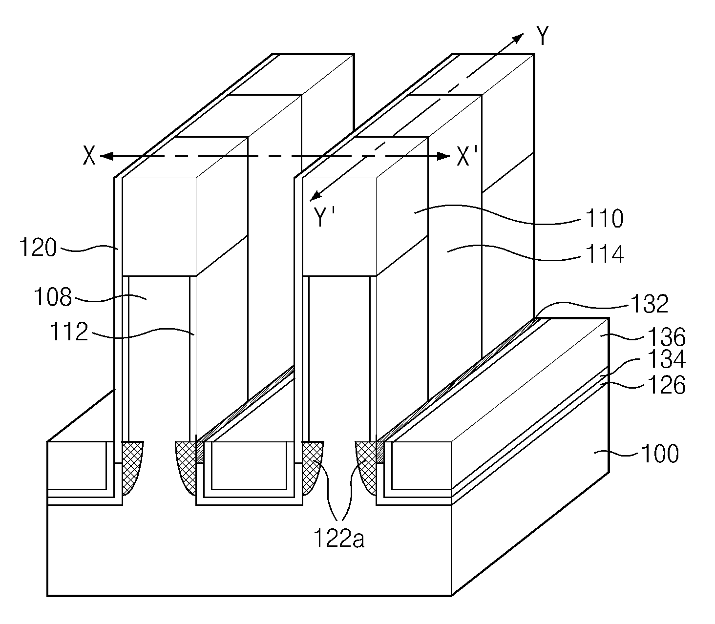
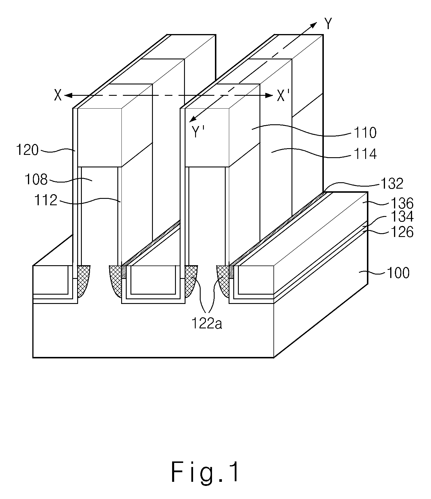
[0030]FIG. 1 is a perspective view of a semiconductor device having a vertical channel transistor according to an embodiment of the present invention.

[0031]Referring to FIG. 1, a hard mask pattern 110 is formed over a pillar 108 that is obtained by etching a silicon substrate 100. A buffer oxide film 112 is formed at a sidewall of the pillar 108. Junction regions 122a doped with impurity ions are formed in the silicon substrate 100 under the pillar 108. A titanium nitride film 134 is formed over a separation oxide film 126, and a tungsten film 136 is formed over the titanium nitride film 134. According to an embodiment of the present invention, the titanium nitride film 134 and the tungsten film 136 form a metal bit line. The bit line may be formed as high as the junction region 122a. The separation oxide film 126 separates the metal bit line from the silicon subs...


PUM


Abstract

A semiconductor device having a vertical channel transistor and a method for manufacturing the same are provided. In the semiconductor device, a metal bit line is formed between vertical channel transistors, and the metal bit line is connected to only one of the vertical channel transistors through an asymmetric bit line contact. Through such a structure, the resistance of the bit line can be improved and the process margin for formation of the bit line can be secured.

Description

CROSS-REFERENCE TO RELATED APPLICATION[0001]The priority of Korean patent application No. 10-2009-0046864 filed on May 28, 2009, the disclosure of which is hereby incorporated in its entirety by reference, is claimed.BACKGROUND OF THE INVENTION[0002]The present invention relates to a semiconductor device having a vertical channel transistor, and more particularly, to a semiconductor device which is capable of using an entire space (width) between vertical channel transistors as a bit line region, without separating the space.[0003]As the integration of semiconductor devices has increased, the channel length of transistors has gradually shrank. The reduction of the channel length causes a short channel effect, such as a drain induced barrier lowering (DIBL), a hot carrier effect, and a punch through.[0004]To solve those shortcomings, various methods have been proposed. One exemplary method is to reduce a depth of a junction region or to increase a channel length by forming a recess c...

Claims


Application Information

Patent Timeline
IPC IPC(8): H01L29/78H01L21/336
CPCH01L29/7827H01L29/66666H01L21/02244H01L29/78642H01L29/78696H10B12/482
Inventor SUNG, MIN CHUL
Owner SK HYNIX INC
Why Eureka
Try Eureka