Silicon epitaxial wafer and manufacturing method thereof

a technology of silicon epitaxial wafers and manufacturing methods, applied in the direction of polycrystalline material growth, crystal growth process, chemically reactive gases, etc., can solve the problems of particle generation in the device manufacturing process, damage to the substrate's back surface, etc., to achieve the yield ratio of wafer manufacturing or even device manufacturing, and easy removal

Active Publication Date: 2010-12-30
SHIN-ETSU HANDOTAI CO LTD
View PDF4 Cites 10 Cited by
  • Summary
  • Abstract
  • Description
  • Claims
  • Application Information

AI Technical Summary

Benefits of technology

[0015]In view of the above-described problem, it is an object of the present invention to provide a silicon epitaxial wafer and a manufacturing method thereof that can reduce particle generation in a device manufacturing process.
[0018]When the substrate having the silicon oxide film on the back main surface excluding the edge portion of the substrate is placed on the susceptor through the silicon oxide film to form the epitaxial layer in this manner, the epitaxial layer can be grown without generating contact scratches by the susceptor on at least the edge portion of the substrate and the region that is 1 mm inside from the outer periphery of the back main surface or the entire back surface, and the particle generation from the substrate can be suppressed in a subsequent process. Therefore, a yield ratio of wafer manufacture or subsequent device manufacture and a quality can be improved.
[0020]When the silicon substrate contains the dopant in this manner, autodoping from the back surface of the silicon substrate can be suppressed during the growth of the epitaxial layer by restricting the silicon oxide film to be removed to the region extending at most 1 mm from the outer periphery toward the inner side of the back main surface.
[0022]As described above, the silicon oxide film on the edge portion can be accurately removed by mirror polishing, and the silicon epitaxial wafer with no particle generation can be manufactured when the edge portion of the silicon substrate is the mirror finished surface.
[0024]When the silicon oxide film is formed on the entire back surface of the silicon substrate by the CVD method in this manner, the CVD silicon oxide film can be readily formed, and the silicon oxide film can be easily removed after growing the epitaxial layer.
[0025]The silicon epitaxial wafer and the manufacturing method thereof according to the present invention can grow the epitaxial layer without contact scratches generated due to the susceptor on the back surface of the silicon substrate, and the particle generation from the substrate can be suppressed in a subsequent process. Therefore, a yield ratio of wafer manufacture or even device manufacture and a quality of a wafer product can be improved.

Problems solved by technology

However, this kind of susceptor comes into contact with the substantially entire back surface of the substrate, and hence it has a problem that a placing surface (the back surface) of the substrate is damaged.
Further, when scratches remain on the back surface of the substrate, they become a cause of particle generation in a subsequent device manufacturing process.
However, although such a type of susceptor does not damage the entire back main surface of the substrate, but it supports the substrate at a part alone, and hence there is a problem that a scratch at a contact portion is deep, the substrate bends or slip occurs from the edge portion of the substrate.
However, even though the ingenuity is exercised with respect to the substrate supporting method in this manner, the problem of particle generation in the device manufacturing process still arises.

Method used


Image

  • Silicon epitaxial wafer and manufacturing method thereof
  • Silicon epitaxial wafer and manufacturing method thereof
  • Silicon epitaxial wafer and manufacturing method thereof

Examples


example

[0064]The present invention will now be more specifically explained based on examples and comparative examples according to the present invention, but the present invention is not restricted thereto.

examples 1 and 2

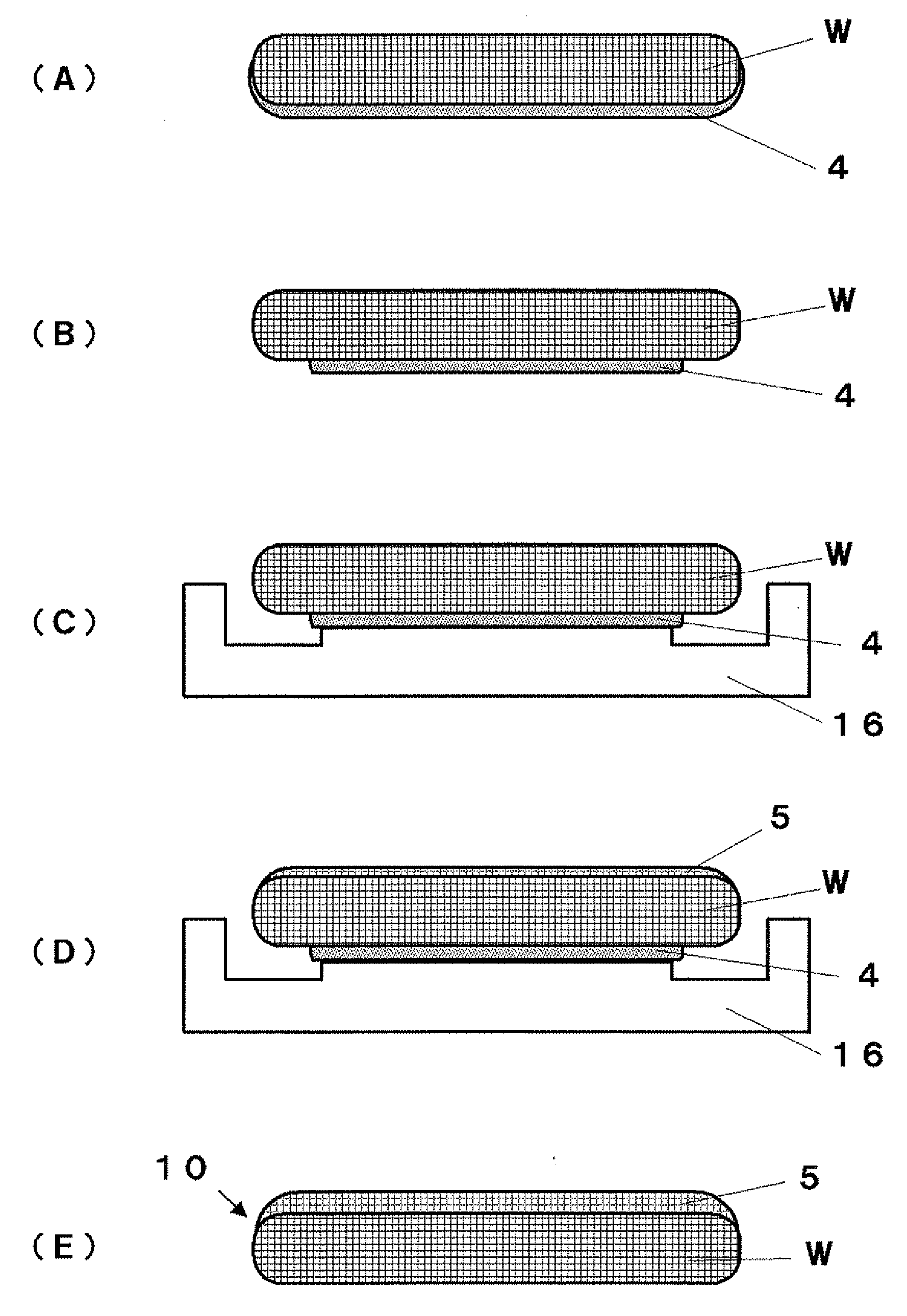
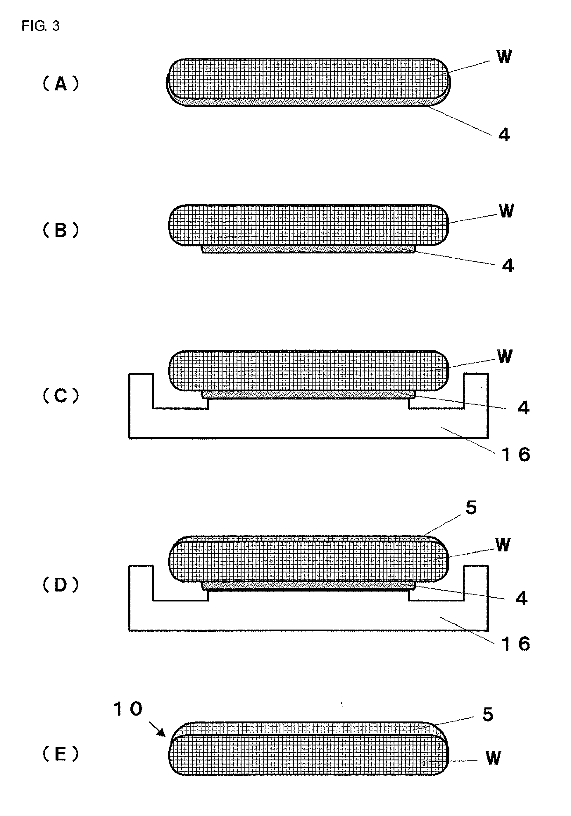
[0065]Each silicon epitaxial wafer was manufactured in a flow depicted in FIG. 3.

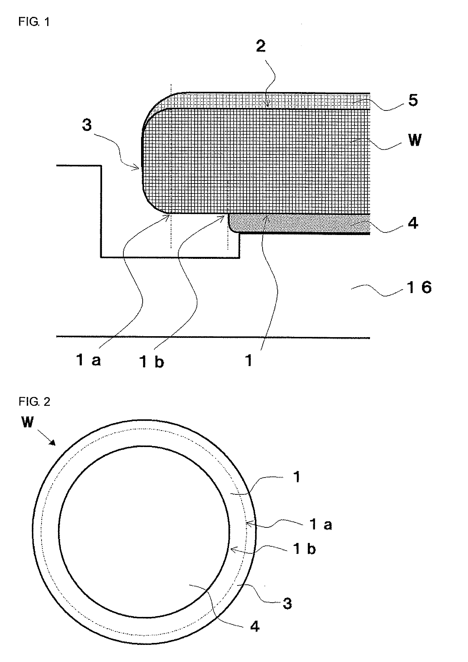
[0066]First, a silicon single crystal substrate having an edge portion 3 with a width of 0.5 mm which is formed of p-type boron-doped (6×10¹⁸ atoms / cm3) p+ silicon single crystal having a diameter of 300 mm was prepared as a substrate W. At this time, a back main surface 1 of the substrate W has a diameter of 299 mm.

[0067]Then, a CVD silicon oxide film having a thickness of 3500 Å (350 nm) was formed on the entire back surface of the silicon substrate W by the CVD method at a normal pressure.

[0068]Subsequently, the CVD oxide film formed on an edge portion and a region extending 1 mm from an outer periphery of the back main surface toward an inner side of the substrate was removed by mirror polishing. Therefore, a diameter of the CVD oxide film 4 formed on the back main surface of the substrate became approximately 297 mm.

[0069]Then, the silicon substrate W was placed on a susceptor 16 through the silico...


PUM

PropertyMeasurementUnit
diameteraaaaaaaaaa
temperatureaaaaaaaaaa
widthaaaaaaaaaa

Abstract

Provided is a method for manufacturing a silicon epitaxial wafer by growing an epitaxial layer by placing a silicon substrate on a susceptor. The method includes at least a step of forming a silicon oxide film entirely on the rear surface of the silicon substrate; a step of removing the silicon oxide film formed at least on an edge section of the silicon substrate; and a step of placing the silicon substrate on the susceptor with the silicon oxide film in between. An epitaxial layer is grown on the silicon substrate, while holding the silicon substrate by the susceptor with the silicon oxide film in between. Thus, the silicon epitaxial wafer by which generation of particles can be reduced in a device manufacturing process and a method for manufacturing such silicon epitaxial wafer are provided.

Description

TECHNICAL FIELD[0001]The present invention relates to a method for manufacturing a silicon epitaxial wafer by placing a substrate on a susceptor and growing a silicon epitaxial layer in an epitaxial growth apparatus and to a silicon epitaxial wafer manufactured by this method.BACKGROUND ART[0002]An epitaxial growth technology is a technology for epitaxially growing a single-crystal thin film layer in vapor phase, which is utilized in manufacture of an integrated circuit such as a bipolar transistor or an MOSLSI, and it is a very important technology since a uniform single crystal thin film can be grown on a clean semiconductor single crystal substrate in accordance with a crystal orientation of the substrate or a precipitous impurity gradient of a junction having a large dopant concentration difference can be formed.[0003]As apparatuses that perform such epitaxial growth, three types, i.e., a vertical type (a pancake type), a barrel type (a cylinder type) and a lateral type are gene...

Claims


Application Information

Patent Timeline
Patent Type & Authority Applications(United States)
IPC IPC(8): H01L29/30H01L21/20
CPCC30B25/20C30B29/06H01L21/68735H01L21/02532H01L21/02658H01L21/02381
Inventor ARAI, TAKESHI
Owner SHIN-ETSU HANDOTAI CO LTD
Why Eureka
Try Eureka