Method for Fabricating Butt-Coupled Electro-Absorptive Modulators

a technology of electro-absorptive modulators and butt-coupled electrodes, which is applied in the field of optical modulators, can solve the problems of increasing scattering loss

Inactive Publication Date: 2010-12-30
BAE SYST INFORMATION & ELECTRONICS SYST INTERGRATION INC
View PDF62 Cites 62 Cited by
  • Summary
  • Abstract
  • Description
  • Claims
  • Application Information

AI Technical Summary

Problems solved by technology

Since germanium-silicon based material system has a relatively high index contrast and its single mode dimension is very small (the single mode cut-off dimension is less than 1 μm), it is a big challenge to achieve an efficient waveguide-modulator coupling.
Another problem is that standard reactive ion etching (RIE) of germanium-silicon based material usually results in rough sidewalls that increases the scattering loss in the germanium-silicon based electro-absorptive modulator.

Method used


Image

  • Method for Fabricating Butt-Coupled Electro-Absorptive Modulators
  • Method for Fabricating Butt-Coupled Electro-Absorptive Modulators
  • Method for Fabricating Butt-Coupled Electro-Absorptive Modulators

Examples


Embodiment Construction

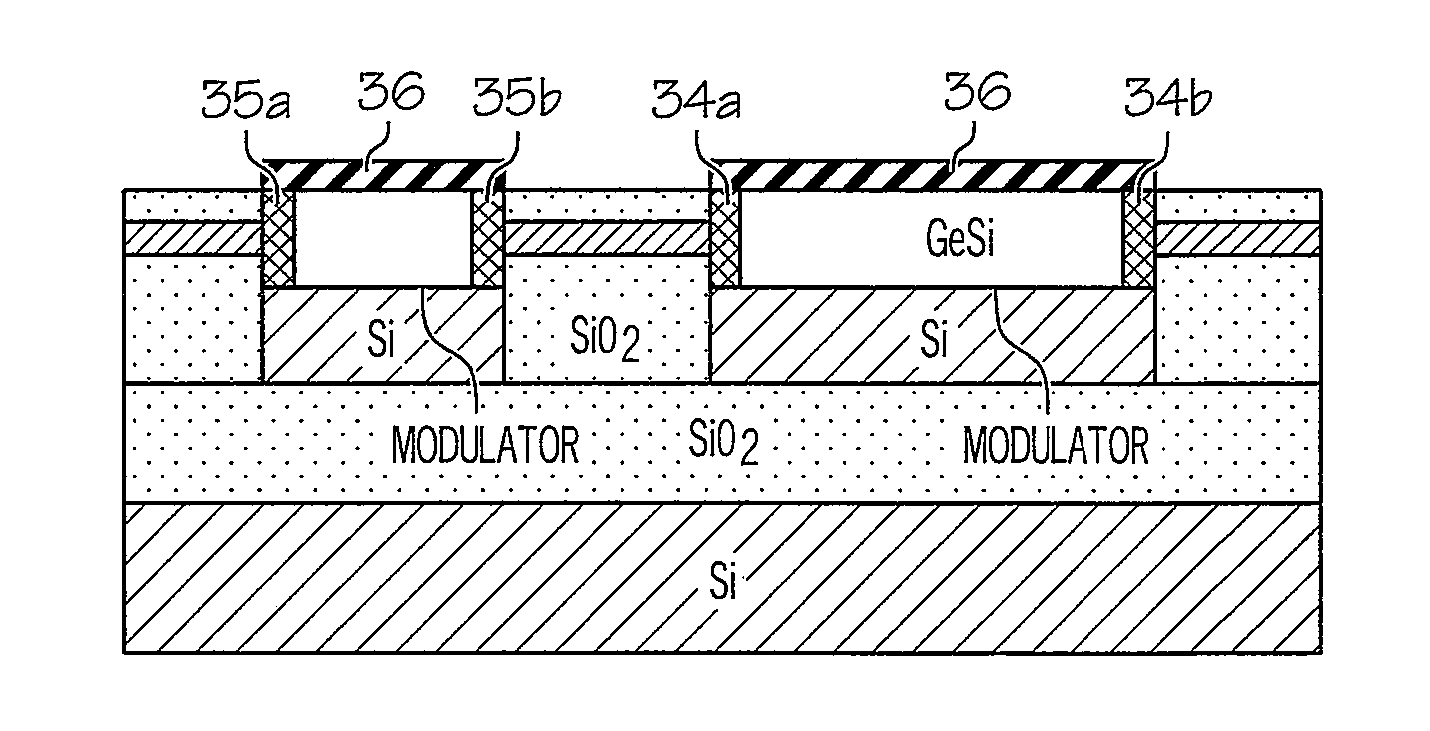
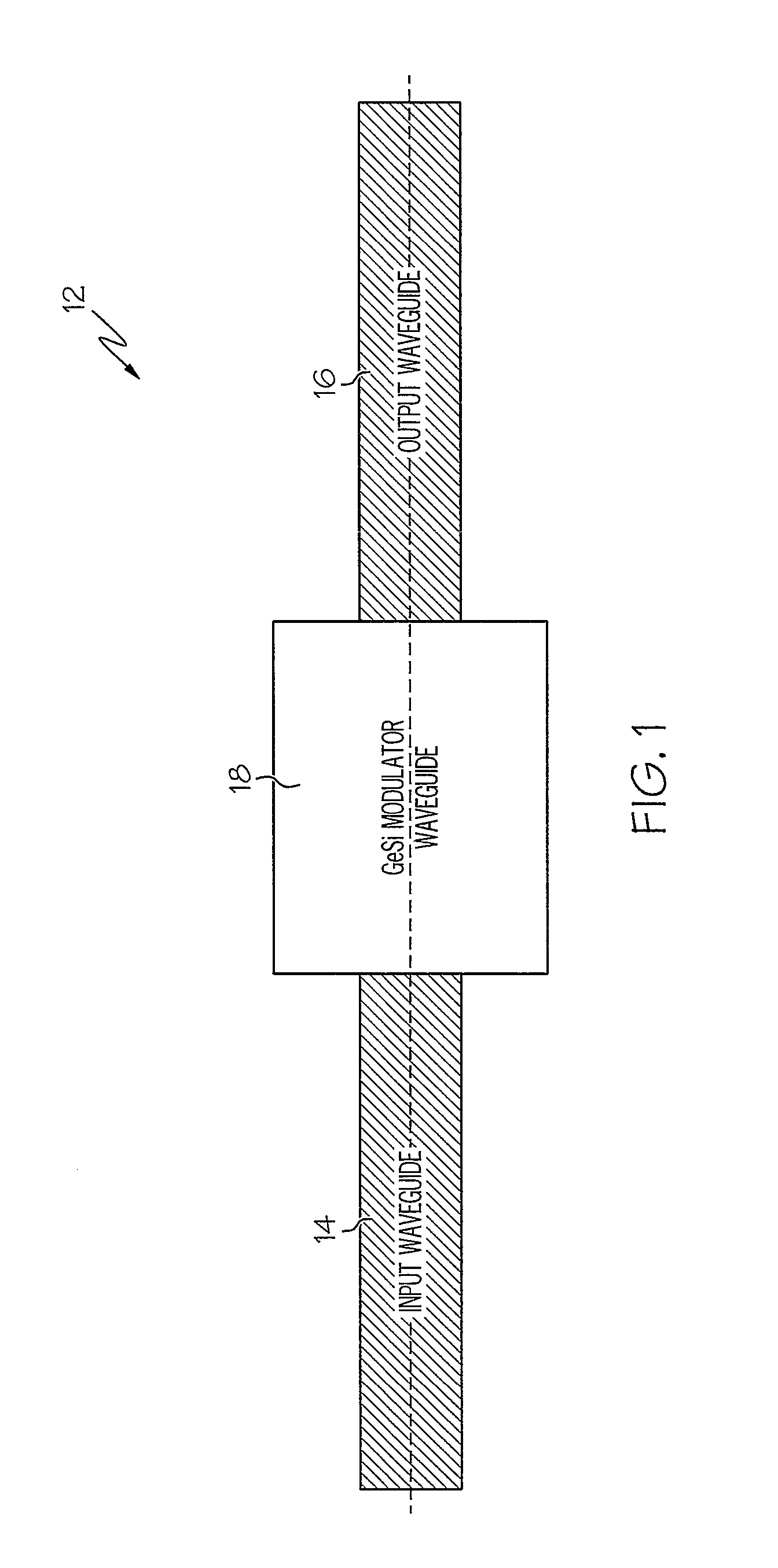
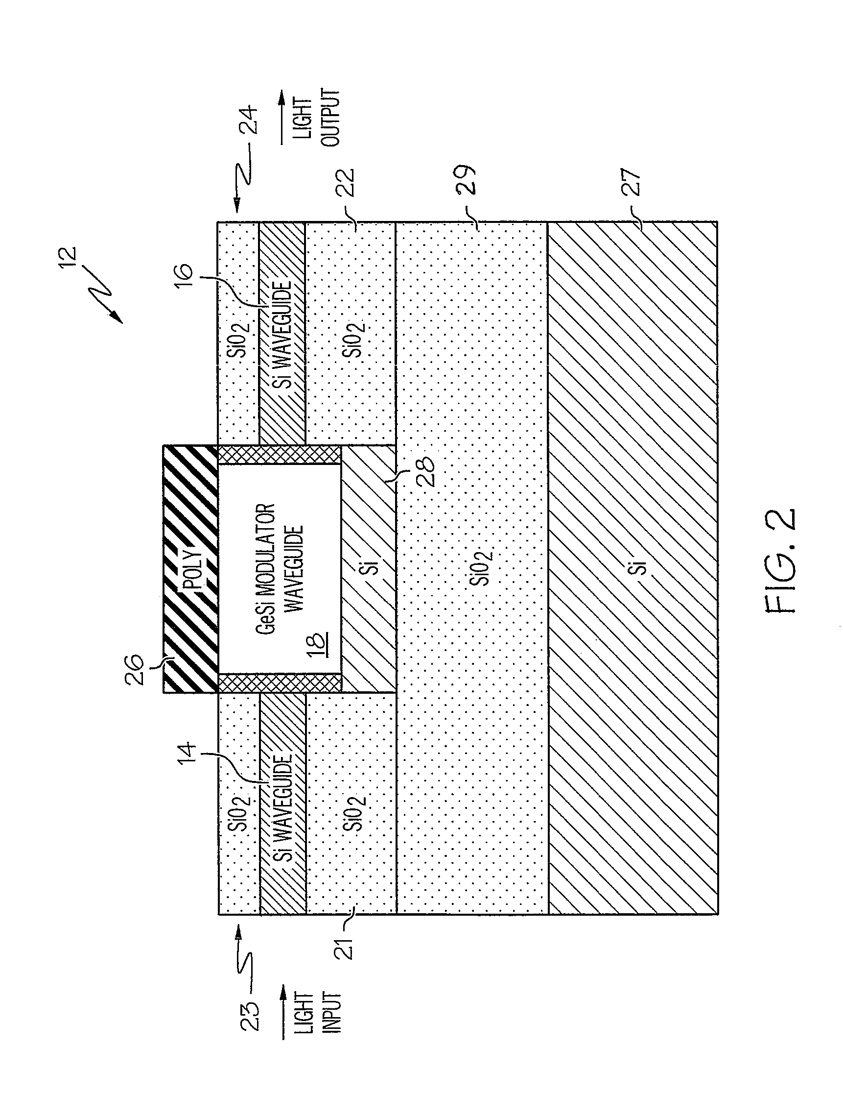
[0015]Referring now to the drawings and in particular to FIG. 1, there is illustrated a high-level block diagram of a germanium-silicon based electro-absorptive optical modulator. As shown, an optical modulator 12 includes an input waveguide 14, an output waveguide 16, and a modulator waveguide 18. Modulator waveguide 18 provides active light modulation between input waveguide 14 and output waveguide 16. Input waveguide 14 and output waveguide 16 are silicon (Si) waveguides. Modulator waveguide 18 can be made of germanium (Ge) or germanium-silicon (GeSi). The composition of the GeSi material is chosen such that the relative change in the absorption coefficient at a voltage-on state compared to a voltage-off state is maximized around the operating wavelength. The voltage-off state of modulator waveguide structure 18 is operated at a relatively low absorption regime of the GeSi material, and the length of modulator waveguide 18 is less than the order of ˜150 μm so as to keep a low abs...


PUM

PropertyMeasurementUnit
lengthaaaaaaaaaa
thicknessesaaaaaaaaaa
transmissionaaaaaaaaaa

Abstract

A method for fabricating butt-coupled electro-absorptive modulators is disclosed. A butt-coupled electro-absorptive modulator with minimal dislocations in the electro-absorptive material is produced by adding a dielectric spacer for lining the coupling region before epitaxially growing the SiGe or other electro-absorptive material. It has been determined that during the SiGe growth, the current process has exposed single crystal silicon at the bottom of the hole and exposed amorphous silicon on the sides. SiGe growth on the amorphous silicon is expected to have more dislocations than single crystal silicon. There should also be dislocations or fissures where the SiGe growth from the each nucleation source finally join. Thus, a dielectric sidewall can protect an exposed waveguide face from any etching from an aggressive surface preparation prior to epi growth.

Description

PRIORITY CLAIM[0001]The present application claims benefit of priority under 35 U.S.C. §365 to the previously filed international patent application number PCT / US08 / 74800 filed on Aug. 29, 2008, assigned to the assignee of the present application, and having a priority date of Oct. 30, 2007, based upon U.S. provisional patent application No. 61 / 001,161. The contents of both applications are incorporated herein by reference.STATEMENT OF GOVERNMENT INTEREST[0002]The present invention was made with United States Government assistance under Contract No. HR0011-05-C-0027 awarded by Defense Advanced Research Projects Agency (DARPA). The United States Government has certain rights in the present invention.BACKGROUND OF THE INVENTION[0003]1. Technical Field[0004]The present invention relates to optical modulators in general, and in particular to a method for fabricating butt-coupled electro-absorptive modulators.[0005]2. Description of Related Art[0006]Silicon-based modulators are commonly ...

Claims


Application Information

Patent Timeline
Patent Type & Authority Applications(United States)
IPC IPC(8): H01L31/0232H01L31/18
CPCG02F1/025
Inventor HILL, CRAIG M.POMERENE, ANDREW T.S.
Owner BAE SYST INFORMATION & ELECTRONICS SYST INTERGRATION INC
Why Eureka
Try Eureka