Test access control apparatus and method thereof

a technology of access control and stacked chips, which is applied in the direction of resistance/reactance/impedence, testing circuits, instruments, etc., can solve the problems of high expectations for the technology, the high cost of available tsv for 3d-ic testing, and the severe problem of exponential decay in quality of stacked dies employed in such technologies. , to achieve the effect of better ensuring the yield of stacked chip devices

Inactive Publication Date: 2010-12-30
NATIONAL TSING HUA UNIVERSITY
View PDF5 Cites 82 Cited by
  • Summary
  • Abstract
  • Description
  • Claims
  • Application Information

AI Technical Summary

Benefits of technology

[0007]The present invention provides a test access control apparatus and method for stacked chip devices that can perform System On Chip (SOC

Problems solved by technology

However, the stacked dies employed in such technologies will face the severe problem of exponential decay in quality if the currently employed post-bond testing technique is not changed.
However, the available TSV for 3D-IC

Method used


Image

  • Test access control apparatus and method thereof
  • Test access control apparatus and method thereof
  • Test access control apparatus and method thereof

Examples


Embodiment Construction

[0013]The present invention will be explained with the appended drawings to clearly disclose the technical characteristics of the present invention.

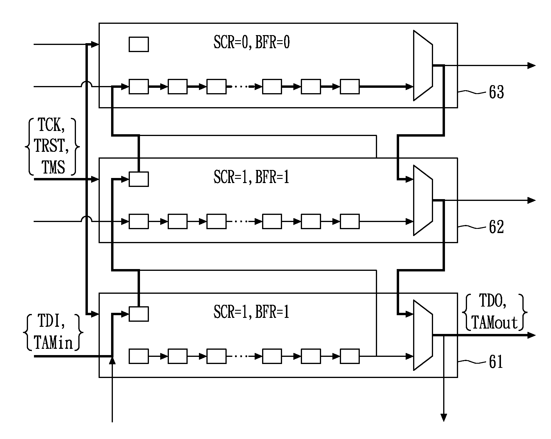
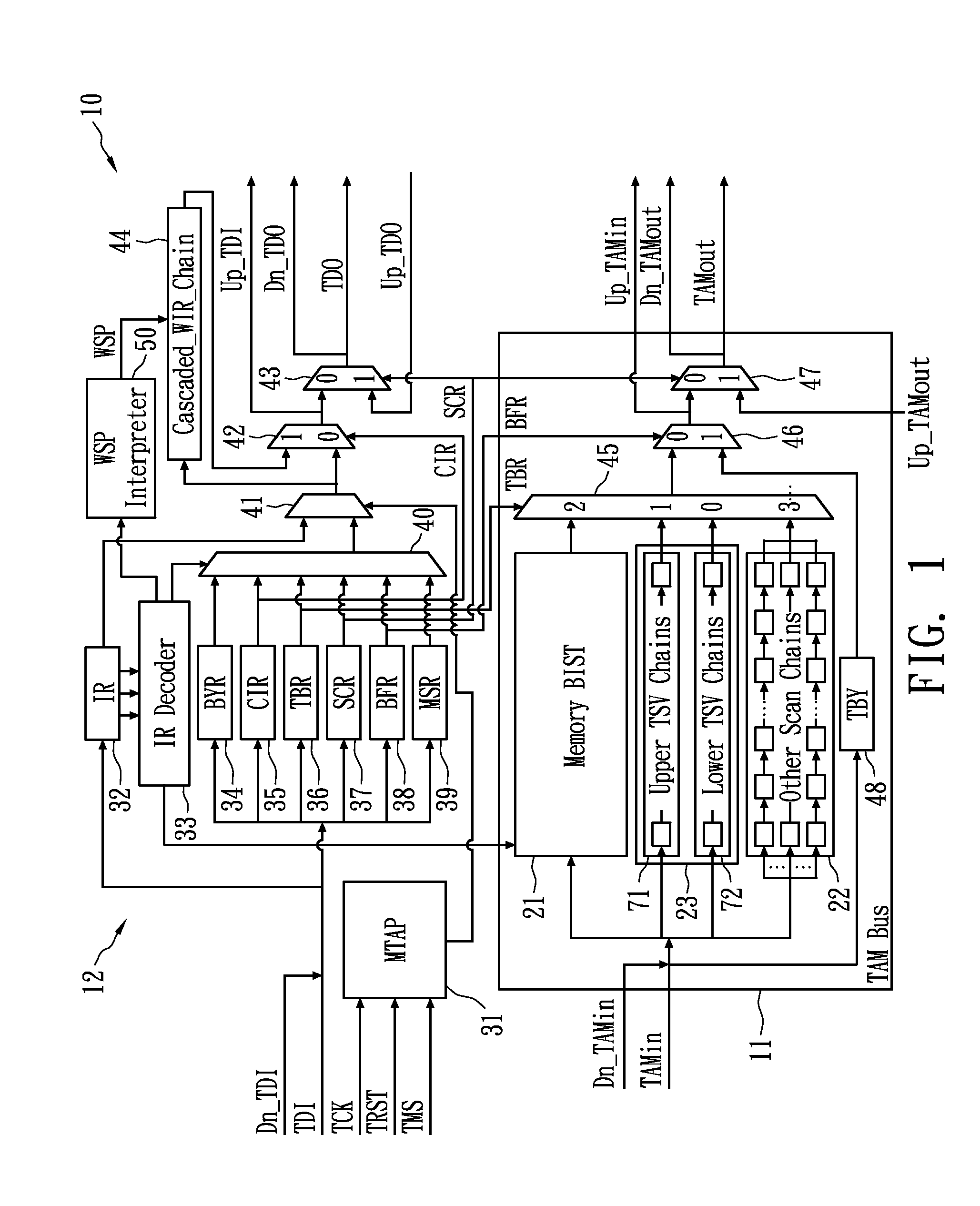
[0014]FIG. 1 shows a test access control apparatus for testing a stacked chip device (3D-IC) in accordance with an embodiment of the present invention. The stacked chip device comprises at least a first chip layer (lower chip layer) and a second chip layer (upper chip layer). Each layer of 3D-IC will implement a test access control apparatus. A test access control apparatus 10 includes test access mechanism (TAM) buses 11 and an extended IEEE 1149.1 Test Access Port (TAP) Controller 12. The TAM buses 11 support related test control and / or test instructions to memory built-in-self-test (BIST) circuit 21 for the memory known-good-die (KGD) test, scan chains 22 for the logic KGD test; and through-silicon-via (TSV) chains 23 that are configured to conduct the TSV test that verifies any defect in vertical interconnects between any two chip la...


PUM


Abstract

A test access control apparatus includes test access mechanism (TAM) buses and an extended IEEE 1149.1 Test Access Port (TAP) Controller. The TAM buses support memory built-in-self-test (BIST) circuit for the memory known-good-die (KGD) test, scan chains for the logic KGD test; and through-silicon-via (TSV) chains that are configured to conduct the TSV test that verifies any defect in vertical interconnects between any two chip layers of the stacked chip device. The TAP Controller is coupled to the TAM buses and is configured to control the memory KGD test, the logic KGD test and the TSV test between two chip layers. A cost-effective connection or configuration of test access control apparatus in 3D-IC is also present. In accordance with an embodiment of the present invention, a test access control method includes a yield-concerned test methodology for 3D-IC, and an integrated flow of test access control apparatus supporting heterogeneous test protocols of SOC

Description

BACKGROUND OF THE INVENTION[0001](A) Field of the Invention[0002]The present invention is related to a test access control apparatus and method for a stacked chip device.[0003](B) Description of the Related Art[0004]Three-dimensional (3D) integration or wafer-to-wafer or chip-to-chip bonding technology has been considered the most promising solution to extend the life of Moore's law in semiconductor manufacturing technology. However, the stacked dies employed in such technologies will face the severe problem of exponential decay in quality if the currently employed post-bond testing technique is not changed.[0005]Through-silicon via (TSV) is the latest in a progression of technologies for stacking silicon devices in 3D arrangements. Placing and wiring devices in 3D promises higher clock rates, lower power dissipation, and higher integration density. 3D TSV technology will be adopted in many applications because it solves issues related to electrical performance, memory latency, powe...

Claims


Application Information

Patent Timeline
IPC IPC(8): G01R31/00G06F19/00
CPCG01R31/318513G01R31/318558G11C2029/3202G11C29/32G11C5/02
Inventor WU, CHENG WENLO, CHIH YENHSING, YU TSAO
Owner NATIONAL TSING HUA UNIVERSITY
Why Eureka
Try Eureka