Method of Multi-segments Modeling Bond Wire Interconnects with 2D Simulations in High Speed, High Density Wire Bond Packages

a technology of high density and bond wire, applied in the direction of instrumentation, program control, semiconductor/solid-state device details, etc., can solve the problem that the method cannot avoid the disadvantage of empirical formulae, and achieve fast and accurate bond wire parasitic inductance, cost and design turn-around time greatly reduced

Active Publication Date: 2010-12-30
MARVELL ASIA PTE LTD
View PDF5 Cites 20 Cited by
  • Summary
  • Abstract
  • Description
  • Claims
  • Application Information

AI Technical Summary

Benefits of technology

[0016]In one aspect of the invention, a method is provided for developing a fast and accurate bond wire parasitic inductance and capacitance extraction that builds an equivalent circuit model of the bond wires and delivers a signal noise analysis of an entire package in seconds. The method is advantageously used from early the final stages of the design and serves as a guide to meet design targets and verification. In this way, the cost and turn-around time of design are greatly reduced.

Problems solved by technology

This method cannot avoid the disadvantage of empirical formulae.

Method used


Image

  • Method of Multi-segments Modeling Bond Wire Interconnects with 2D Simulations in High Speed, High Density Wire Bond Packages
  • Method of Multi-segments Modeling Bond Wire Interconnects with 2D Simulations in High Speed, High Density Wire Bond Packages
  • Method of Multi-segments Modeling Bond Wire Interconnects with 2D Simulations in High Speed, High Density Wire Bond Packages

Examples


Embodiment Construction

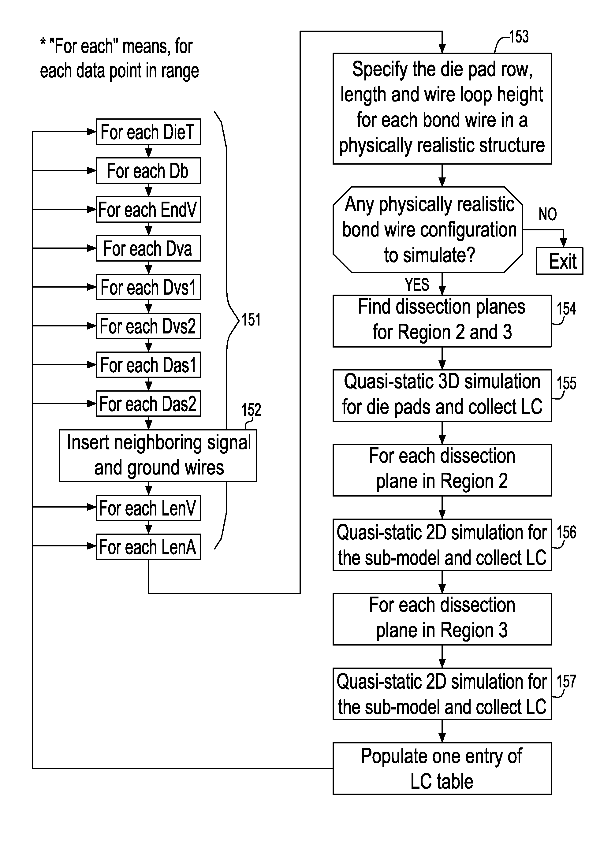
[0038]The present invention provides a fast and relatively accurate bond wire parasitic inductance and capacitance extraction by building an equivalent circuit model of the bond wires.

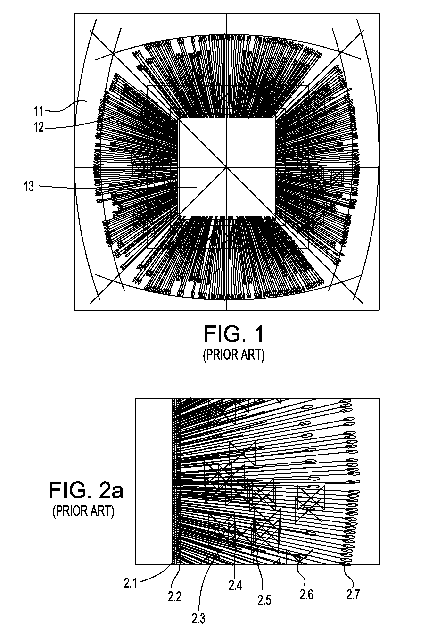
[0039]Die-up (i.e., a chip mounted on top of a package.), Electrically Enhanced Plastic Ball Grid Array (EPBGA) with two rows of bond finger pads and two rows of die pads will be used henceforth only for illustrative purposes. Other suitable types of wire bond chip carriers with in-line or staggered die pads and with one or two rows of bond finger pads can also be used.

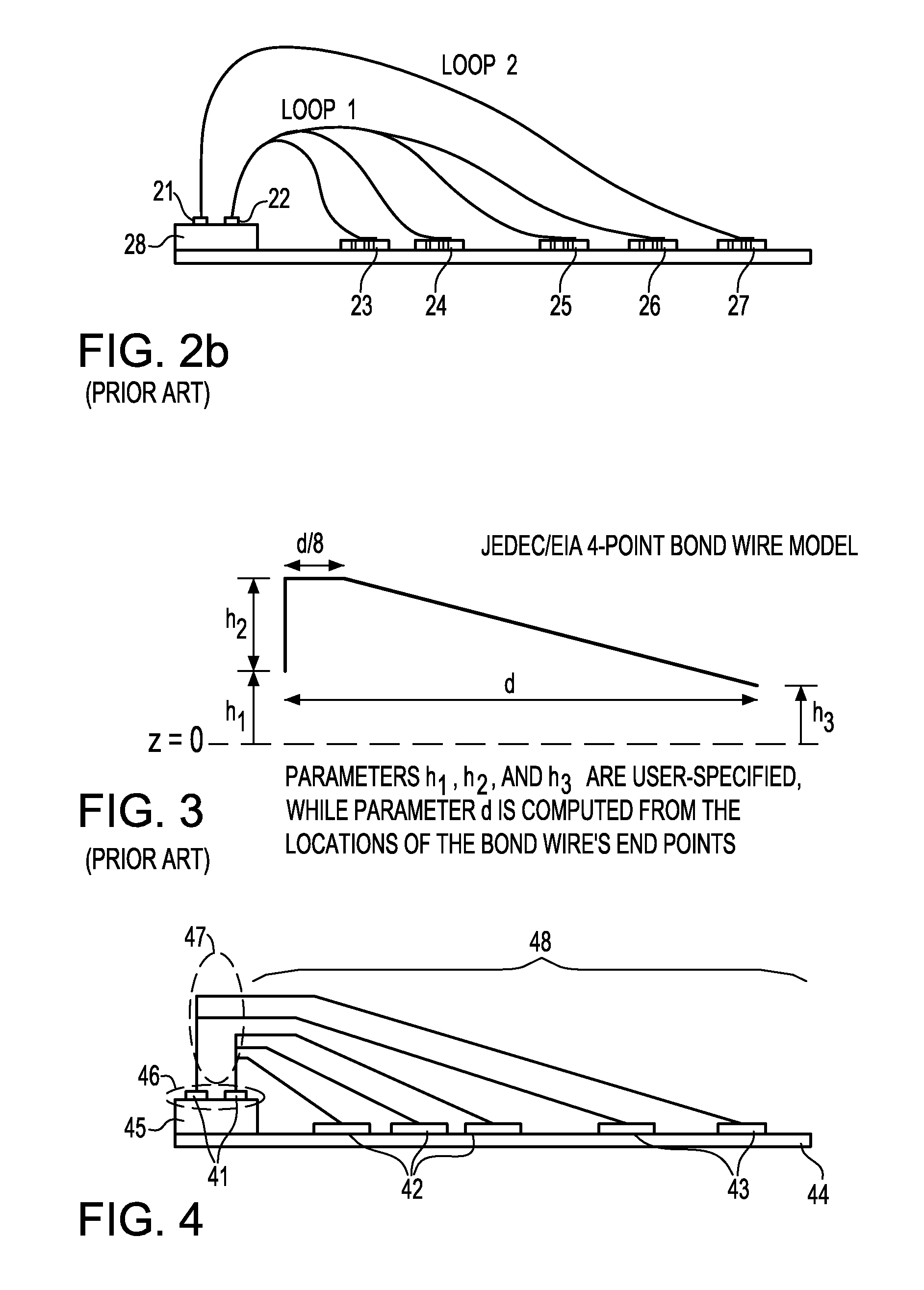
[0040]In a preferred embodiment of the present invention, the modeling method creates a multi-segment equivalent circuit model consisting of LC values of each segment for a victim-aggressor pair. The modeling method achieves accurate results by factoring important factors affecting the EM field between victim and aggressor wires, including couplings between victim and aggressor wires, couplings from other signal wires, ground shields, po...


PUM


Abstract

A method for modeling bond wires in an IC package for predicting noise effects generated by electromagnetic coupling in complex bond wire configurations. A look-up table of equivalent LC circuit models for the bond wires is generated that accurately predicts the effects of the bond wire circuitry of a signal transmission system. Switch and mirror techniques are applied to reduce the bond wire configurations necessary to simulate. The method includes: setting parameters related to the IC package layout of groups of bond wires; sub-dividing each group of bond wires into regions, each including a portion of the bond wire or its corresponding pad, and generating dissection planes for the regions consisting of the bond wires; performing a 3D simulation on the regions consisting of the corresponding pads, and a 2D simulation for each dissection plane; constructing equivalent circuit models for groups of bond wires and corresponding pads based on the 3D and 2D simulations results; inputting the equivalent circuit models into a circuit simulator to measure the noise effects; and modifying the layout geometry to meet noise targets.

Description

FIELD OF THE INVENTION[0001]The present invention relates to the Design Automation of Integrated Circuit packages, and more particularly, to electromagnetic modeling and extracting electrical parasitics of bond wire interconnects in advanced wire bond packages of semiconductor chips.BACKGROUND OF THE INVENTION[0002]It is known in the art that chips are typically mounted in or on wire bond packages. Electrical signal propagation and power transportation between chips and packages are through bond wires which connect the wires on the chips to the wires in the packages. Compared with its traditional counterpart, advanced wire bond package technology has a denser bond wire layout and higher speed. It pushes the application space into Gbps, which is comparable to but less expensive than other package technologies, such as High Performance Glass ceramic (HPGC) package technology, alumina ceramic package technology and organic flip-chip Plastic Ball Grid Array (FCPBGA) package technology.[...

Claims


Application Information

Patent Timeline
Patent Type & Authority Applications(United States)
IPC IPC(8): G06F17/50
CPCG06F17/5036H01L2924/01006H01L24/06H01L24/48H01L24/49H01L2224/4809H01L2224/48091H01L2224/48095H01L2224/484H01L2224/49171H01L2224/49173H01L2924/09701H01L2924/14H01L2924/30105H01L2924/30107H01L2924/3025H01L2224/05554H01L2224/48227H01L2924/01076H01L2924/01055H01L2924/01033H01L2924/01023H01L2924/01005H01L23/552H01L2924/00014H01L2924/00G06F30/367H01L2224/45099H01L2224/05599
Inventor HU, HAITIANBUDELL, TIMOTHY W.CHIU, CHARLES S.TREMBLE, ERIC
Owner MARVELL ASIA PTE LTD
Why Eureka
Try Eureka