Eureka AIR delivers breakthrough ideas for toughest innovation challenges, trusted by R&D personnel around the world.

Insulating substrate and method for producing the same

a technology of insulating substrate and substrate, which is applied in the direction of clayware, manufacturing tools, and semiconductor/solid-state device details, etc., can solve the problems of reducing heat radiation performance, affecting durability, and failure to exhibit sufficient heat radiation performance, so as to enhance heat radiation performance, excellent thermal conductivity, and excellent electrical conductivity

Inactive Publication Date: 2011-01-13
SHOWA DENKO KK
View PDF1 Cites 9 Cited by
  • Summary
  • Abstract
  • Description
  • Claims
  • Application Information

AI Technical Summary

Benefits of technology

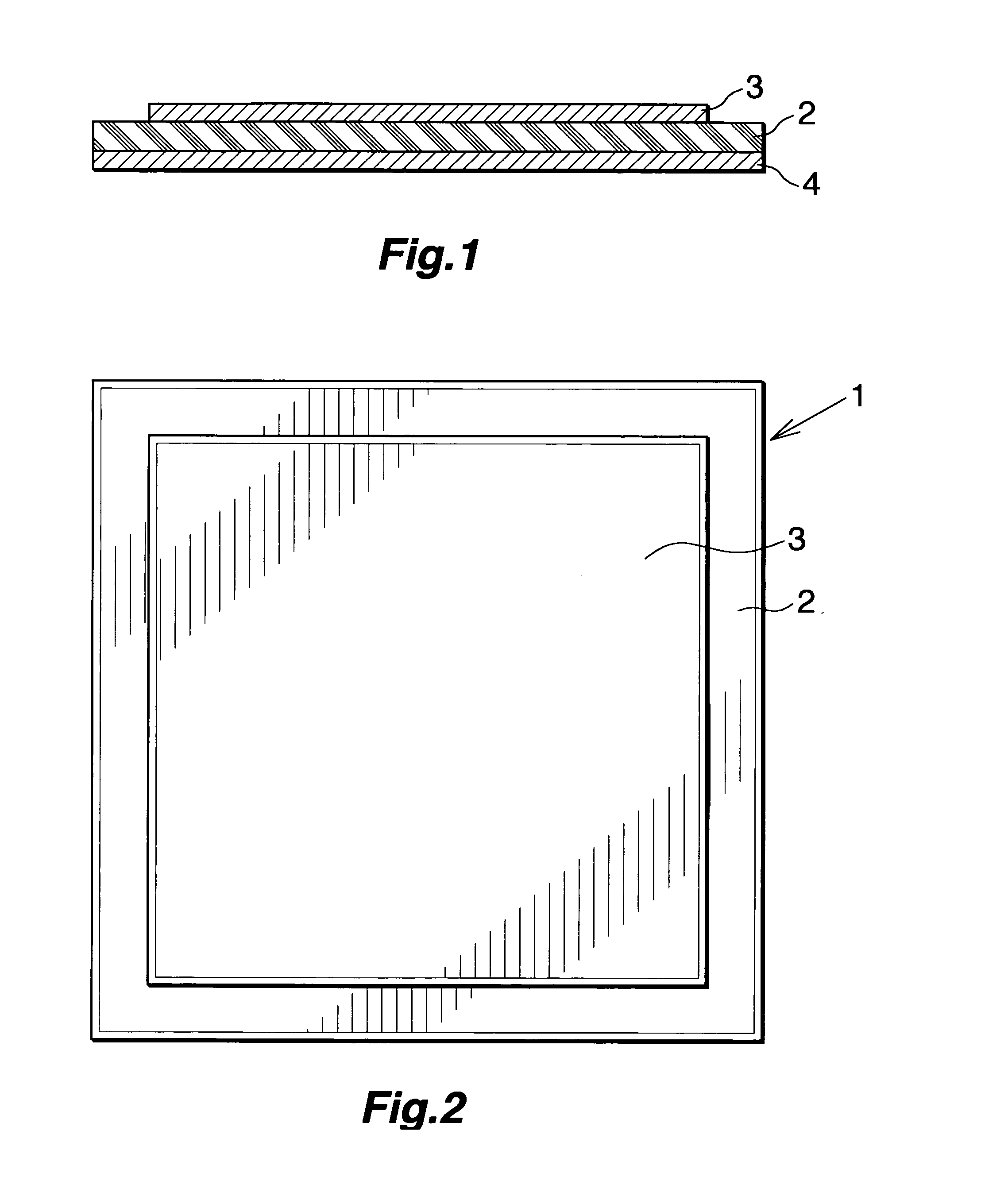
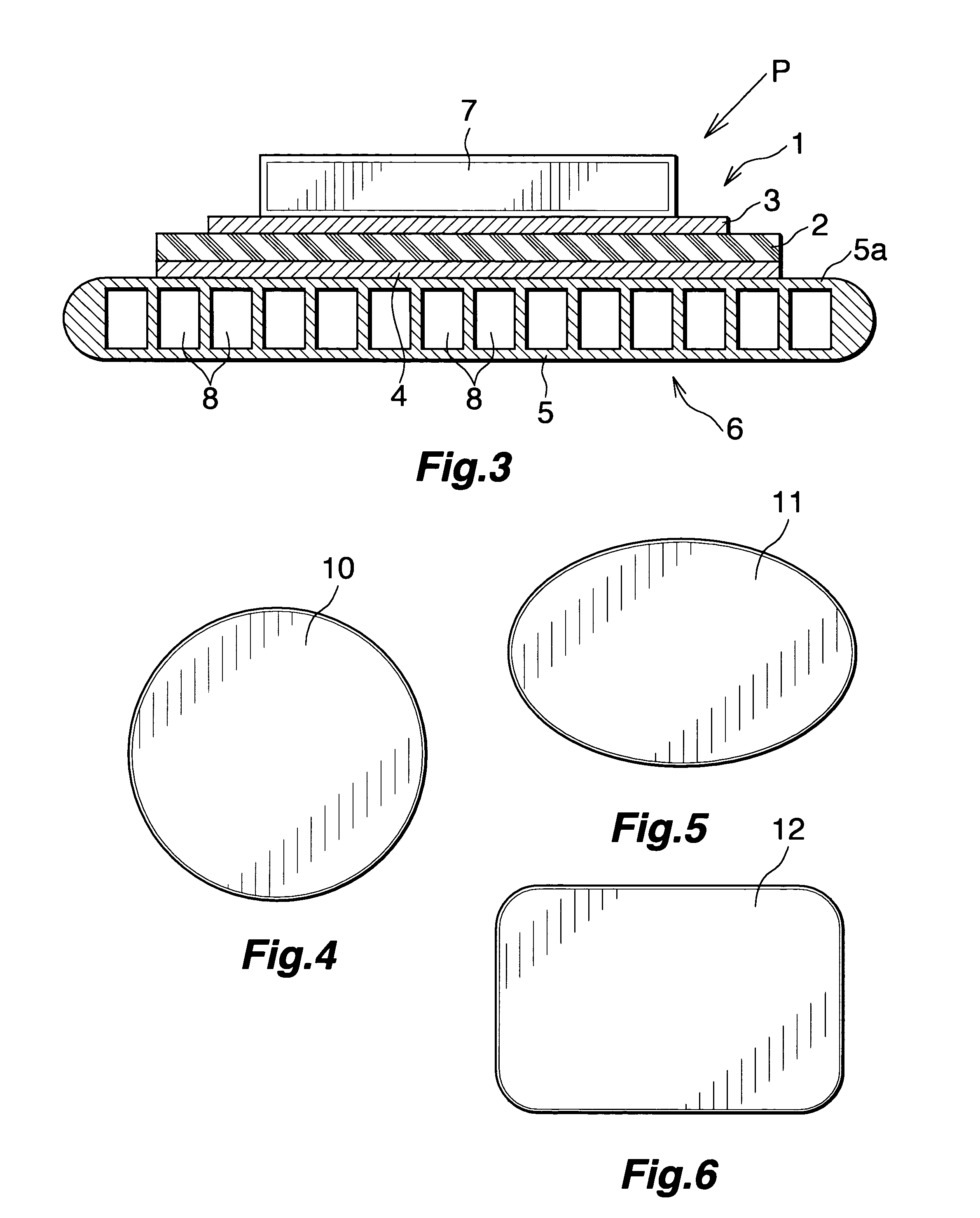
[0025]The insulating substrate of par. 1) is used as follows: the stress relaxation layer of the insulating substrate is joined to a heat sink formed of a high-thermal-conduction material, such as aluminum or copper, through welding or brazing, or bonding by use of a highly heat conductive adhesive, and a power device is mounted on the wiring layer of the power module base, thereby completing a power module. Since only the wiring layer, the electrically insulative layer, and the stress relaxation layer are present between the power device and the heat sink, as compared with a power module which uses the insulating substrate described in Patent Document 1, a heat conduction path from the power device to the heat sink becomes shorter, thereby enhancing radiation performance for heat generated from the power device. Also, since the wiring layer and the stress relaxation layer are spark plasma sintered bodies formed respectively on the electrically insulative layer, there is no need to dispose a brazing material having a low thermal expansion coefficient between the electrically insulative layer and each of the wiring layer and the stress relaxation layer, whereby excellent thermal conductivity is established between the electrically insulative layer and each of the wiring layer and the stress relaxation layer.
[0026]Further, even when thermal stress is generated in the power module base from a phenomenon in which the difference in thermal expansion coefficient between the heat sink and the electrically insulative layer of the insulating substrate causes the heat sink to be pulled by the electrically insulative layer and thus to attempt to warp, the stress relaxation layer functions to relax thermal stress, thereby preventing generation of a crack in the electrically insulative layer and generation of warpage of a joint surface of the heat sink joined to the stress relaxation layer. Therefore, radiation performance is maintained for a long period of time.
[0027]According to the insulating substrate of par. 3), excellent electrical conductivity and excellent thermal conductivity are imparted to the wiring layer.
[0028]According to the insulating substrate of par. 4), excellent thermal conductivity is imparted to the stress relaxation layer. Further, in the case of use of a power module in which a power device is mounted on a power module base which uses the insulating substrate, when thermal stress is generated in the power module base, the stress relaxation layer yields an excellent thermal-stress relaxation effect.
[0029]According to the insulating substrate of par. 5), the following advantageous effect is attained. In the case of use of a power module in which a power device is mounted on a power module base which uses the insulating substrate, when thermal stress is generated in the power module base, the stress relaxation layer yields an excellent thermal-stress relaxation effect.
[0030]In the case of the insulating substrate of any one of pars. 6) to 8), even when thermal stress is generated in the power module base of the above-described power module from a phenomenon in which the difference in thermal expansion coefficient between the heat sink and the electrically insulative layer of the insulating substrate causes the heat sink to be pulled by the electrically insulative layer and thus to attempt to warp, since the external shape of the stress relaxation layer does not have an edge portion where thermal stress is concentrated, separation of the stress relaxation layer and the heat sink can be prevented more reliably.

Problems solved by technology

As a result, generation of a crack in the insulating substrate, separation of joined surfaces, and an impairment in durability arise.
However, in a power module in which a power device is mounted on the wiring layer of the power module base described in Patent Document 1, since the wiring layer, the electrically insulative layer, the heat transfer layer, and the heat radiation substrate are present between the power device and the heat sink, a heat conduction path from the power device to the heat sink becomes long, with a resultant drop in heat radiation performance.
Also, since the heat radiation substrate and the heat sink are merely screwed together, thermal conductivity therebetween is insufficient, resulting in a failure to exhibit sufficient heat radiation performance.

Method used


Image

  • Insulating substrate and method for producing the same
  • Insulating substrate and method for producing the same
  • Insulating substrate and method for producing the same

Examples


example 1

[0057]An AlN powder having an average particle size of 6 μm and produced by an ordinary production method was placed in a die of graphite. A pair of electrodes was disposed in such a manner as to face the interior of the die. Subsequently, in a state in which a uniaxial pressure of 50 MPa was imposed on the AlN powder, spark plasma sintering was performed through application of a pulse current of 2,000 A maximum between the paired electrodes and through retention at a sintering temperature for five minutes, thereby forming the electrically insulative layer (2) having a square shape with 50 mm on sides and a thickness of 0.635 mm. In the above-mentioned spark plasma sintering, sintering temperature for the AlN powder was 1,800° C.

[0058]An Al powder having an average particle size of 100 μm was produced through gas atomizing. The gas-atomized Al powder having an average particle size of 100 μm and an SiC powder having an average particle size of 10 μm produced by an ordinary productio...

example 2

[0061]An AlN powder having an average particle size of 6 μm and produced by an ordinary production method was placed in a die of graphite. A pair of electrodes was disposed in such a manner as to face the interior of the die. Subsequently, in a state in which a uniaxial pressure of 50 MPa was imposed on the AlN powder, spark plasma sintering was performed through application of a pulse current of 1,000 A maximum between the paired electrodes and through retention at a sintering temperature for five minutes, thereby forming the electrically insulative layer (2) having a square shape with 12 mm on sides and a thickness of 0.635 mm. In the above-mentioned spark plasma sintering, sintering temperature for the AlN powder was 1,800° C.

[0062]An Al powder having an average particle size of 100 μm was produced through gas atomizing. The gas-atomized Al powder having an average particle size of 100 μm and an SiC powder having an average particle size of 10 μm produced by an ordinary productio...


PUM

PropertyMeasurementUnit
temperatureaaaaaaaaaa
pressureaaaaaaaaaa
temperatureaaaaaaaaaa

Abstract

An insulating substrate 1 includes an electrically insulative layer 2, a wiring layer 3 formed on one side of the electrically insulative layer 2 and formed of a spark plasma sintered body of an electrically conductive material powder, and a stress relaxation layer 4 formed on the other side of the electrically insulative layer 2 and formed of a spark plasma sintered body of an alloy powder or a mixed powder to be formed into a metal composite. The wiring layer 3 is formed of a spark sintered body of a powder selected from the group consisting of an Al powder, a Cu powder, an Ag powder, and an Au powder. The stress relaxation layer 4 is formed of a spark plasma sintered body of a powder selected from the group consisting of an Al—Si alloy powder, a mixed powder of a Cu powder and an Mo powder, a mixed powder of a Cu powder and a W powder, a mixed powder of an Al powder and an SiC powder, and a mixed powder of an Si powder and an SiC powder. Use of the insulating substrate can yield a power module which can prevent a drop in heat radiation performance and can enhance durability.

Description

TECHNICAL FIELD[0001]The present invention relates to an insulating substrate for mounting thereon, for example, a semiconductor device, and to a method of manufacturing the same.[0002]The term “aluminum” as used herein encompasses aluminum alloys in addition to pure aluminum, except for the case where “pure aluminum” is specified. Needless to say, metal as expressed by an elemental symbol indicates pure metal.BACKGROUND ART[0003]In recent years, in order to control large power, a power module which includes a power device formed of a semiconductor device, such as an IGBT (Insulated Gate Bipolar Transistor), has been widely used. In such a power module, the semiconductor device must be held at a predetermined temperature or lower by means of efficiently radiating heat generated therefrom. A base for a power module (hereinafter referred to as a “power module base”) which meets the requirement has conventionally been proposed (see Patent Document 1). The power module base includes a c...

Claims


Application Information

Patent Timeline
Patent Type & Authority Applications(United States)
IPC IPC(8): H05K1/00H05K1/09C04B35/64
CPCH01L21/4846C04B2237/86H01L23/467H01L23/473H01L2924/0002H01L23/3735C04B2237/408B22F3/105B22F7/06C04B35/581C04B35/645C04B37/021C04B37/026C04B2235/5436C04B2235/666C04B2237/12C04B2237/34C04B2237/343C04B2237/366C04B2237/368C04B2237/401C04B2237/402C04B2237/407H01L2924/00
Inventor UNENO, DAISUKEHISAYUKI, KOJI
Owner SHOWA DENKO KK
Why Eureka
Eureka Blog
Learn More