Multilayer dielectric substrate and semiconductor package

a technology of dielectric substrate and semiconductor, applied in the direction of basic electric elements, resonators, semiconductor devices, etc., can solve the problems of unstable operation of semiconductor devices within the cavity, unstable characteristics of transmission lines, and difficulty in setting, so as to achieve maximum attenuation and absorption effect of resistor, less reflection, and maximum attenuation

Inactive Publication Date: 2011-01-13
MITSUBISHI ELECTRIC CORP
View PDF3 Cites 5 Cited by
  • Summary
  • Abstract
  • Description
  • Claims
  • Application Information

AI Technical Summary

Benefits of technology

[0010]According to the first invention, impedance conversion with less reflection from a cavity, that is, a hollow waveguide to a resistance load can be achieved for the first signal wave and the second signal wave, the frequency thereof being different from that of the first signal wave, by the impedance transformer. Further, an electric field is maximized (an open point) at the coupling aperture by the tip-short-circuited dielectric transmission line. Therefore, maximum attenuation and absorption effects of the resistor can be provided in the signal frequency bands mentioned above. Thus, cavity resonance is reliably suppressed for signal waves of two frequencies and stable operations of a semiconductor device and a transmission line can be obtained.

Problems solved by technology

However, resonance is generated in a frequency band that a size of the cavity determined by a member such as a cover is about ½ or an integer multiple of a free-space propagation wavelength, and thus an operation of the semiconductor device within the cavity and characteristics of transmission lines become unstable.
Therefore, it becomes difficult to set the size of the cavity for accommodating the device to be less than ½ of the propagation wavelength corresponding to the signal frequency, and a high-order resonant mode is likely to be generated.

Method used


Image

  • Multilayer dielectric substrate and semiconductor package
  • Multilayer dielectric substrate and semiconductor package
  • Multilayer dielectric substrate and semiconductor package

Examples


first embodiment

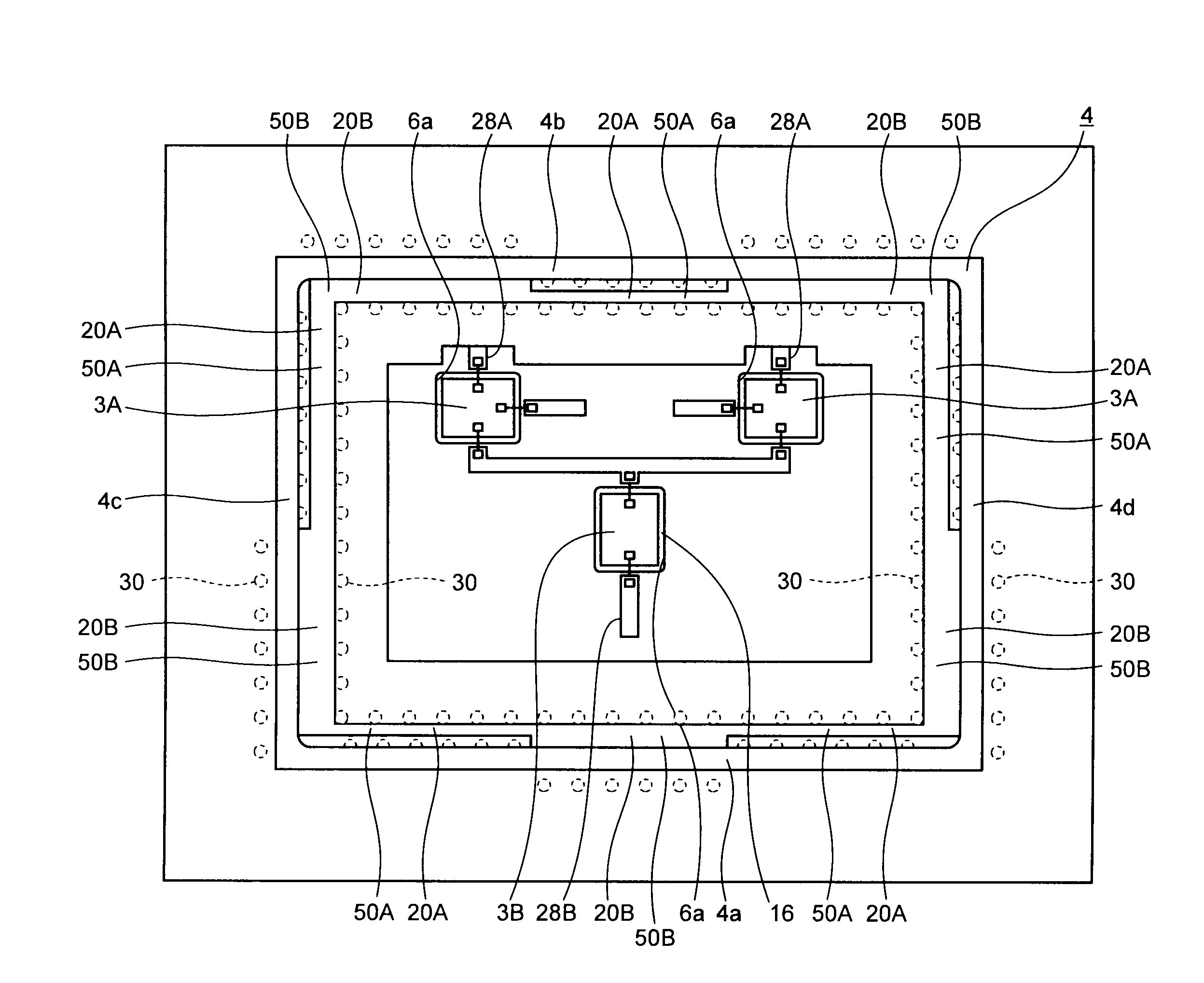
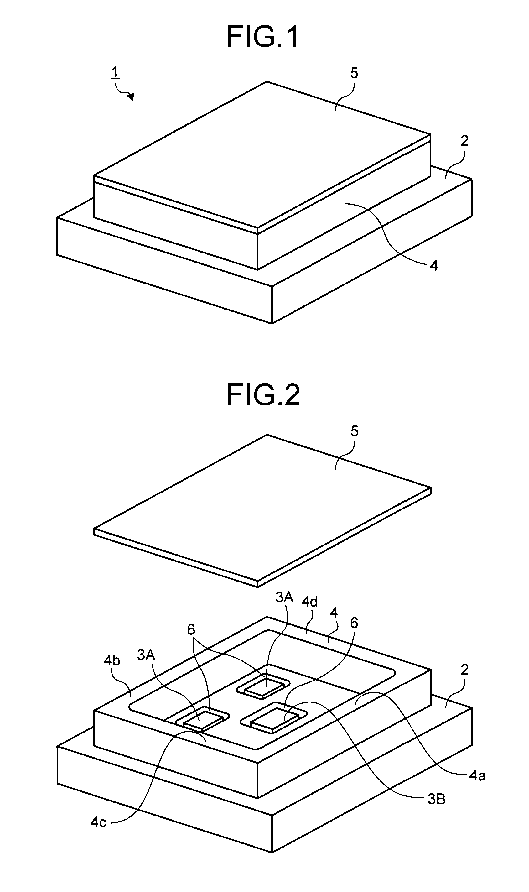
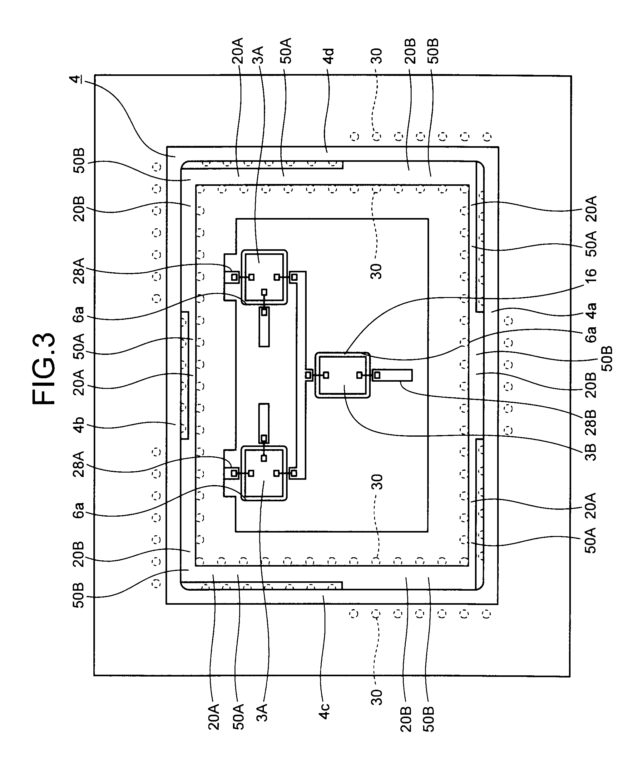
[0057]FIG. 1 is a perspective view of an appearance of the semiconductor package (a high frequency package) according to the present invention. FIG. 2 is a perspective view of an appearance of the semiconductor package according to the present invention with a cover removed. FIG. 3 is a plan view of an internal configuration of the semiconductor package according to the present invention. FIG. 4 is a cross-sectional view of an internal hierarchical structure of a multilayer dielectric substrate of the semiconductor package according to a first embodiment. FIG. 5 is a partial enlarged cross-sectional view in which a first cavity-resonance suppressing circuit shown in FIG. 4 is enlarged. FIG. 6 is a cross-sectional view of the internal hierarchical structure of the multilayer dielectric substrate of the semiconductor package according to the first embodiment. FIG. 7 is a partial enlarged cross-sectional view in which a second cavity-resonance suppressing circuit shown in FIG. 5 is enl...

second embodiment

[0078]FIG. 10 is a partial enlarged cross-sectional view of an internal hierarchical structure of a multilayer dielectric substrate of a semiconductor package according to a second embodiment, particularly depicting a first cavity-resonance suppressing circuit in detail. FIG. 11 is a partial enlarged cross-sectional view of the internal hierarchical structure of the multilayer dielectric substrate of the semiconductor package according to the second embodiment, particularly depicting a second cavity-resonance suppressing circuit in detail. In the present embodiment, the impedance transformer according to the first embodiment is omitted.

[0079]A first cavity-resonance suppressing circuit 21A is described with reference to FIG. 10. The first opening 50A, that is, a ground open pattern is formed at or around a cavity end of a ground pattern 18 as a surface-layer ground conductor on a surface layer (a first layer) of the multilayer dielectric substrate 2. The tip-short-circuited first di...

third embodiment

[0082]FIG. 12 is a partial enlarged cross-sectional view of an internal hierarchical structure of a multilayer dielectric substrate of a semiconductor package according to a third embodiment, particularly depicting a first cavity-resonance suppressing circuit in detail. FIG. 13 is a partial enlarged cross-sectional view of an internal hierarchical structure of the multilayer dielectric substrate of the semiconductor package according to the third embodiment, particularly depicting a second cavity-resonance suppressing circuit in detail.

[0083]In FIG. 12, a first cavity-resonance suppressing circuit 22A is constituted by the first opening 50A, the first impedance transformer 60A, the first coupling aperture 65A, the first dielectric transmission line 80A, and a first resistor via array 30e. That is, in the present embodiment, a resistor is placed between the tip-short-circuited ground via 30d in the dielectric transmission line 80A and the coupling aperture 65A in a direction that the...


PUM


Abstract

A multilayer dielectric substrate includes a first cavity-resonance suppressing circuit that suppresses cavity resonance of a first signal wave and a second cavity-resonance suppressing circuit that suppresses cavity resonance of a second signal wave, a frequency thereof being different from that of the first signal wave. These cavity-resonance suppressing circuits respectively include openings formed in a surface-layer ground conductor, an impedance transformer with a length of an odd multiple of about ¼ of in-substrate effective wavelength of a signal wave, a tip-short-circuited dielectric transmission line with a length of an odd multiple of about ¼, of in-substrate effective wavelength of a signal wave, a coupling aperture formed in an inner-layer ground conductor, and a resistor formed in the coupling aperture. The multilayer dielectric substrate that suppresses cavity resonance of signal waves of a plurality of frequencies.

Description

TECHNICAL FIELD[0001]The present invention relates to a multilayer dielectric substrate on which an electromagnetically shielded space (hereinafter, cavity) for mounting a semiconductor device that operates in a high frequency band such as a microwave band or a millimeter wave band is formed, and relates to a semiconductor package.BACKGROUND ART[0002]In a high frequency package in which a high-frequency semiconductor device that operates in a high frequency band such as a microwave band or a millimeter wave band is mounted, the high-frequency semiconductor device is usually mounted within a cavity that is airtightly and electrically shielded by a cover, a seal ring, and a ground conductor, in view of an environmental resistance and an operational stability.[0003]However, resonance is generated in a frequency band that a size of the cavity determined by a member such as a cover is about ½ or an integer multiple of a free-space propagation wavelength, and thus an operation of the semi...

Claims


Application Information

Patent Timeline
Patent Type & Authority Applications(United States)
IPC IPC(8): H01P7/06
CPCH01L23/055H01L23/12H01L2924/12041H01L2924/15192H01L2224/73265H01L2224/32225H01L24/49H01L24/48H05K1/16H01P5/08H01P3/02H01P1/162H01L23/13H01L23/49822H01L23/49827H01L23/552H01L23/66H01L2224/48091H01L2224/48227H01L2224/49175H01L2924/01004H01L2924/14H01L2924/1423H01L2924/15153H01L2924/1517H01L2924/16195H01L2924/3011H01L2924/3025H01L2924/00014H01L2924/00H01L2924/00012H01L2924/30111H01L2924/12036H01L24/73H01L2224/45099H01L2224/45015H01L2924/207
Inventor YASOOKA, KOUSUKE
Owner MITSUBISHI ELECTRIC CORP
Why Eureka
Try Eureka